Method of fabricating conductive anti-reflection film for a cathode ray tube

a technology of anti-reflection film and cathode ray tube, which is applied in the manufacture of tubes/lamp screens, optical elements, instruments, etc., can solve the problems of high investment cost of the machine, adversely affecting the electronic unit disposed therearound, and inability to prevent aef from taking pla

Inactive Publication Date: 2001-02-06
KK TOSHIBA
View PDF27 Cites 8 Cited by
  • Summary
  • Abstract
  • Description
  • Claims
  • Application Information

AI Technical Summary

Problems solved by technology

In recent years, it is pointed out that an electromagnetic wave generated in the vicinity of an electron gun and a deflection yoke of a Cathode ray tube used in TV sets and computers leaks out and may adversely affect an electronic unit disposed therearound.
However, with such a surface resistance, the AEF cannot be prevented from taking place.
Since the gas phase method requires a large scaled machine for forming a conductive film, the investment cost for the machine is high.
In addition, this method is not suitable for quantitative fabrication.
However, generally, even if a film containing metal particles is thin, it absorbs visible light.
When a conductive film is composed of only metal particles without a binder, since the bond force of the metal particles is insufficient, the film hardness becomes low.
Thus, sufficient conductivity cannot be obtained.
However, since the refractive index and reflectivity of the conductive layer containing metal particles are high, only with the light absorbing characteristics of the light absorbing substance, it is difficul...

Method used


Image

  • Method of fabricating conductive anti-reflection film for a cathode ray tube
  • Method of fabricating conductive anti-reflection film for a cathode ray tube
  • Method of fabricating conductive anti-reflection film for a cathode ray tube

Examples


first and second embodiments

0.5 g of particles of a silver compound such as Ag.sub.2 O, AgNO.sub.3, or AgCl was solved with 100 g of water. Thus, a first solution was prepared. 5% by weight of 3-glycidoxypropyltrimethoxysilane was added to a silicate solution composed of 8 parts by weight of methyl silicate, 0.03 parts by weight of nitric acid (conq), 500 parts by weight of ethanol, and 15 parts by weight of water. Thus, a second solution was prepared. Likewise, 30% by weight of 3-glycidexypropyltrimethoxysilane was added to a silicate solution composed of 8 parts by weight of methyl silicate, 0.03 parts by weight of nitric acid (conq), 500 parts by weight of ethanol, and 15 parts by weight of water. Thus, a third solution was prepared.

Thereafter, the outer surface of a face panel (17-inch panel) of a cathode ray tube that has been assembled was buffed with cerium oxide so as to remove dust and oil. Next, the first solution was coated as a first coat film on the outer surface of the face panel of the cathode r...

third and fourth embodiments

5% by weight of heptadecafluorodecyltrimethoxysilane as solid content equivalent to SiO.sub.2 as shown in Table 2 was added to a silicate solution composed of 8 parts by weight of methyl silicate, 0.03 parts by weight of nitric acid (conq), 500 parts by weight of ethanol, and 15 parts by weight of water. Thus, a first solution was prepared. Likewise, 30% by weight of heptadecafluorodecyltrimethoxysilane as solid content equivalent to SiO.sub.2 as shown in Table 2 was added to a silicate solution composed of 8 parts by weight of methyl silicate, 0.03 parts by weight of nitric acid (conq), 500 parts by weight of ethanol, and 15 parts by weight of water. Thus, a second solution was prepared.

Next, as with the first embodiment, each of the first and second solutions was coated on the first coat film formed on the outer surface of the face panel (17-inch panel) by the spin coat method in the same manner as the first embodiment. Thereafter, the first and second coat films were sintered at ...

first embodiment

As compared examples, each of third and fourth solutions of which heptadecafluorodecyltrimethoxysilane is added as solid content equivalent to SiO.sub.2 as shown in Table 2 was coated on the first coat film by the spin coat method in the same manner as the Thus, second coat films corresponding to the third and fourth solutions were formed. Thereafter, corresponding to the third and fourth solutions, the first and second coat films were sintered at a temperature of 210.degree. C. for 30 minutes.

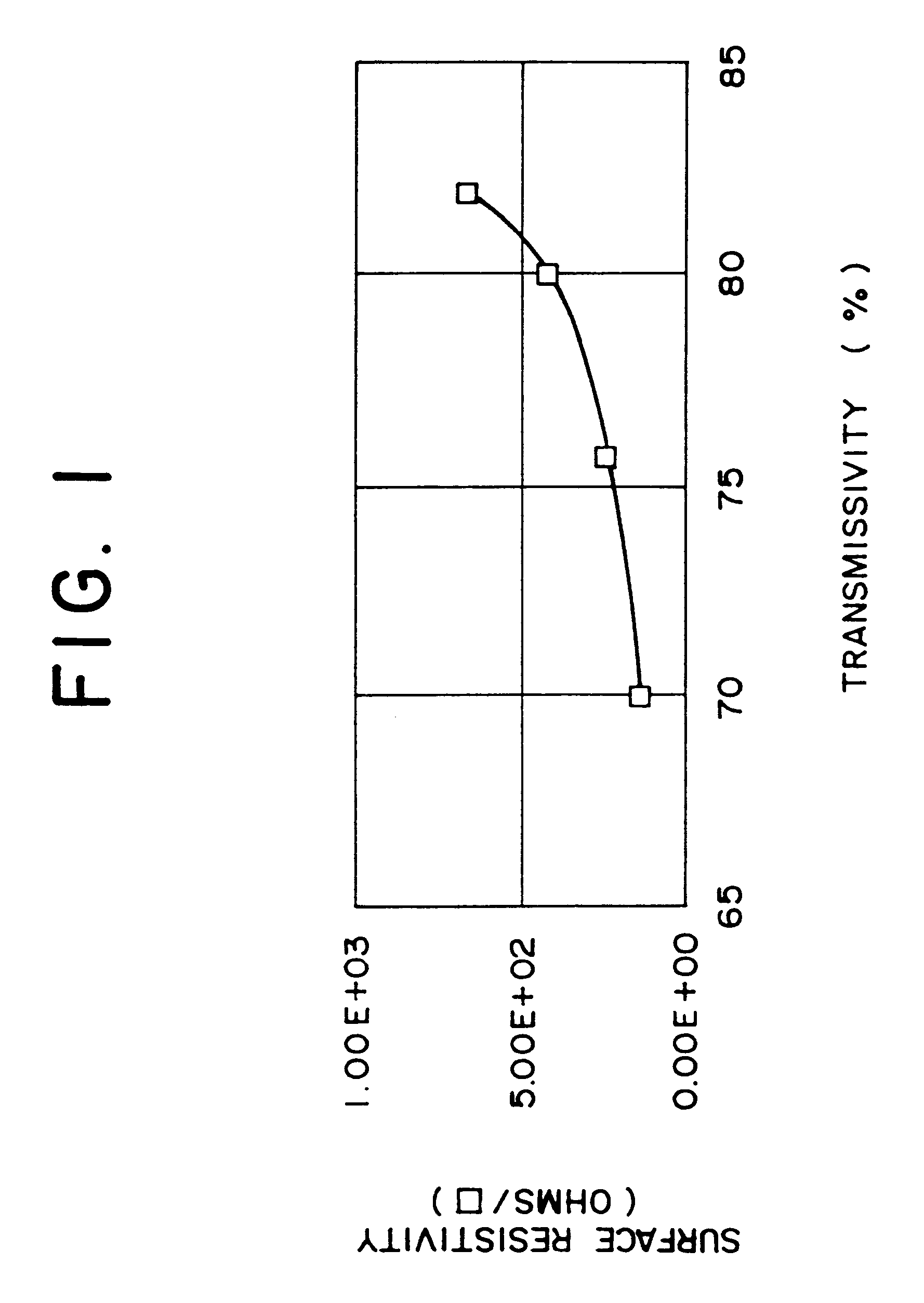
Next, the panel resistance, surface resistance, and film hardness of the conductive anti-reflection films according to the third and fourth embodiments and the fourth and fifth compared examples were measured in the same manner as the first embodiment. In addition, a hot water dipping test and a chemical resistance test for these conductive anti-reflection films were performed. In the hot water dipping test, after the face panel was dipped in tap water at a temperature of 80.degree. C. for 60...


PUM

PropertyMeasurementUnit
Temperatureaaaaaaaaaa
Pressureaaaaaaaaaa
Lengthaaaaaaaaaa

Abstract

A second coat film is formed on a first coat film containing a conductive substance, the second coat film having an expansion coefficient almost the same as the expansion coefficient of the first coat film under a sintering condition. The first and second coat films are sintered at the same time. Thus, a conductive anti-reflection film with sufficiently low surface resistance, excellent water resistance and chemical resistance, and reduced reflected light can be obtained. When the conductive anti-reflection film is used, a cathode ray tube that is almost free from the AEF (Alternating Electric Field) and that displays a high quality picture for a long time can be obtained.

Description

1. Field of the InventionThe present invention relates to a conductive anti-reflection film that functions as an anti-reflection film and protects an AEF (Alternating Electric Field) from taking place, a fabrication method thereof, and a cathode ray tube having the conductive anti-reflection film formed on an outer surface of a face panel of a face plate.2. Description of the Related ArtIn recent years, it is pointed out that an electromagnetic wave generated in the vicinity of an electron gun and a deflection yoke of a Cathode ray tube used in TV sets and computers leaks out and may adversely affect an electronic unit disposed therearound.To prevent the cathode ray tube from leaking out the electromagnetic wave (electric field), it is necessary to decrease the surface resistance of the face panel thereof. In other words, Japanese Patent Laid-Open Application Nos. 61-118932, 61-118946, and 63-160140 disclose various surface treatment methods for preventing a face panel from being st...

Claims


Application Information

Patent Timeline
IPC IPC(8): H01J29/86G02B1/111G02B1/11G02B1/14H01J9/20H01J29/88H01J29/89
CPCH01J29/868H01J29/896H01J2229/8913H01J29/02
Inventor CHIGUSA, HISASHIABE, MICHIYOAOKI, KATSUYUKI
Owner KK TOSHIBA
Why Eureka
Try Eureka