Laser irradiation process

a laser irradiation and laser technology, applied in the direction of crystal growth process, gel state, polycrystalline material growth, etc., can solve the problems of uneven grain size, poor uniform crystal structure of polycrystalline silicon film, and inability to provide satisfactory polycrystalline structur

Inactive Publication Date: 2001-02-13
GOLD CHARM LTD
View PDF7 Cites 208 Cited by
  • Summary
  • Abstract
  • Description
  • Claims
  • Application Information

AI Technical Summary

Problems solved by technology

These processes, however, have a common problem that a crystal structure in a polycrystalline silicon film formed is poorly uniform.
In other words, there occurs unevenness in a grain size due to change in a crystal structure caused by the beam end.
On the other hand, if the absolute value of the energy density slope is too large, an energy density in the boundary region may be decreased too much to provide a satisfactory polycrystalline structure.
If it is less than 1 .mu.m, it is difficult to provide a polycrystalline semiconductor structure in which a grain size is about 1 .mu.m.

Method used


Image

  • Laser irradiation process
  • Laser irradiation process
  • Laser irradiation process

Examples


example 1

The first example of this invention will be described. An amorphous silicon film was formed as follows.

A glass substrate was an OA-2 substrate (Nippon Denki Glass). On the substrate was deposited a silicon dioxide film as a base insulating film 100 nm of thickness by a plasma CVD using SiH.sub.4 and N.sub.2 O, on which was then deposited an amorphous silicon film 75 nm of thickness by a low pressure CVD using Si.sub.2 H.sub.6 under the conditions that a flow rate of Si.sub.2 H.sub.6 was 150 sccm, a pressure was 8 Pa, a substrate temperature was 450.degree. C. and a deposition duration was 70 min.

As a preliminary experiment for determining a profile, an E.sub.p was observed when a pulse laser beam with a wavelength of 308 nm and a pulse width of 50 nm was irradiated on the amorphous silicon film. FIG. 11 shows dependency of an average grain size in a polycrystal structure on an energy density when one pulse laser beam was irradiated on the amorphous silicon film or a polycrystalline ...

example 2

The second example of this invention will be described. A glass substrate was an OA-2 substrate (Nippon Denki Glass). On the substrate was deposited a silicon dioxide film as a base insulating film 100 nm of thickness by a plasma CVD using SiH.sub.4 and N.sub.2 O.

On the substrate was then deposited an amorphous silicon film 50 nm of thickness by a low pressure CVD using Si.sub.2 H.sub.6 under the conditions that a flow rate of Si.sub.2 H.sub.6 was 150 sccm, a pressure was 8 Pa, a substrate temperature was 450.degree. C. and a deposition duration was 46 min.

A preliminary experiment indicated that when the film thickness was 50 nm, E.sub.a and E.sub.p for a pulse laser beam with a wavelength of 308 nm and a pulse width of 50 nm were 420 and 470 mJ / cm.sup.2, respectively.

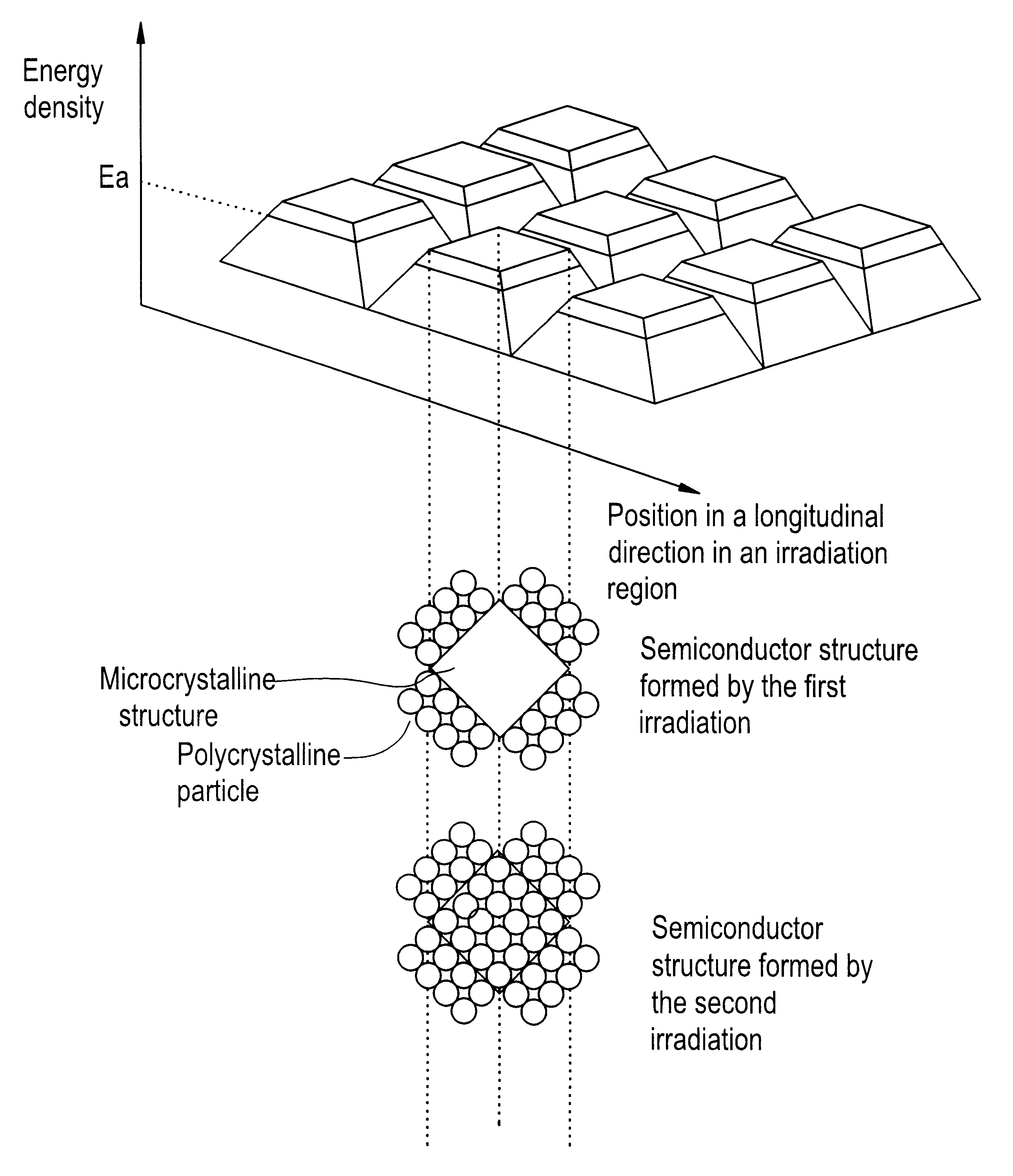
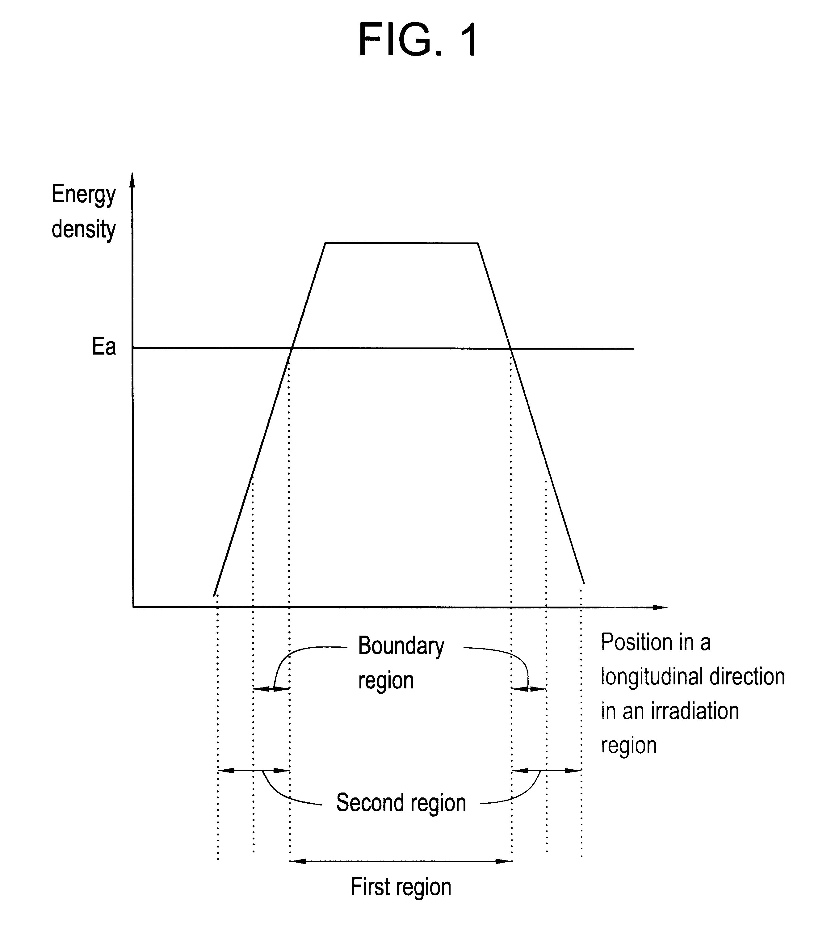
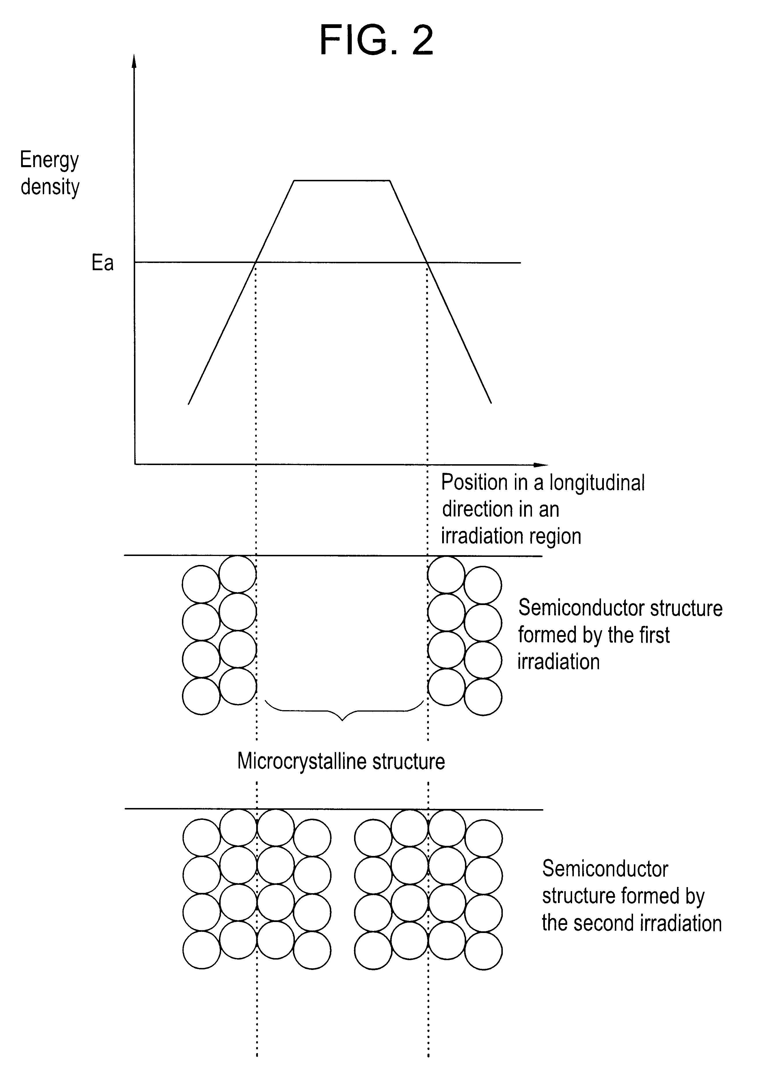
In the light of the results, a beam profile having a shape as shown in FIG. 3 was chosen in this example, and the maximum energy density, the width of the first region with an energy density of E.sub.a or higher, the w...

example 3

The third example of this invention will be described. In this example, energy profiles in both longitudinal and transverse directions in a beam irradiation region met given conditions.

A glass substrate was a 1737 substrate (Corning). On the substrate was deposited a silicon dioxide film as a base insulating film 100 nm of thickness by a plasma CVD using SiH.sub.4 and N.sub.2 O.

On the substrate was then deposited an amorphous silicon film 75 nm of thickness by a plasma CVD using SiH.sub.4 and H.sub.2 under the conditions that a flow rate of SiH.sub.4 was 150 sccm, a flow rate of H.sub.2 was 400 sccm, a pressure was 100 Pa, a discharge power was 0.1 W / cm.sup.2, a substrate temperature was 320.degree. C. and a deposition duration was 8 min. After deposition, the product was subject to dehydro-annealing at 400.degree. C. for 2 hours. When using a pulse laser beam with a wavelength of 248 nm and a pulse width of 35 nm, E.sub.a and E.sub.p for the amorphous silicon film were 480 and 550 ...


PUM

PropertyMeasurementUnit
energy densityaaaaaaaaaa
widthaaaaaaaaaa

Abstract

A pulse laser beam having a rectangular irradiation region is irradiated on the same point in a non-single crystal semiconductor film multiple times. The pulse laser beam has an energy profile in a longitudinal direction in the beam irradiation region as follows: (a) there are the first region having an energy density of Ea or higher and the second regions on both sides of the first region having an energy density of less than Ea, and (b) an energy density slope has an absolute value of 20 to 300 J/cm3 in a boundary region extending to 1 mum from the boundary line between the first and the second regions.

Description

REFERENCE TO RELATED APPLICATION AND INCORPORATION BY REFERENCEThis application is based on application NO.HEI10-219200 filed in Japan, the content of which is incorporated hereinto by reference.1. Field of the InventionThis invention relates to a laser irradiation process comprising irradiating a pulse laser beam on a non-single crystal semiconductor film for annealing; in particular it relates to a laser irradiation process for forming a channel layer in a polycrystalline silicon thin film transistor which may be, for example, used for a liquid crystal display or a contact type image sensor.2. Description of the Related ArtRecently, a thin film transistor comprising a polysilicon film as a channel layer on a glass substrate has been intensely developed for application in, for example, a liquid crystal display or a contact type image sensor. A laser annealing has been a common technique for preparing a polysilicon film in the light of reduction in a process temperature and improvem...

Claims


Application Information

Patent Timeline
Patent Type & Authority Patents(United States)
IPC IPC(8): H01L21/02H01L21/20H01S5/30H01L21/268
CPCH01L21/2026H01L21/0262H01L21/02686H01L21/02678H01L21/02488H01L21/02422H01L21/02532H01L21/02595H01S5/30
Inventor OKUMURA, HIROSHI
Owner GOLD CHARM LTD
Why Eureka
Try Eureka