Formation of punch inspection masks and other devices using a laser

Inactive Publication Date: 2001-03-27
IBM CORP
View PDF13 Cites 13 Cited by
  • Summary
  • Abstract
  • Description
  • Claims
  • Application Information

AI Technical Summary

Benefits of technology

is to provide inexpensive and cost effective inspection masks having a special pattern thereon made by a laser process to enable the user of the mask to easily and ef

Problems solved by technology

This is a time consuming, labor intensive and costly process.
This process is expensive and it requires a relatively long time to make each mask.
The article discusses forming these type masks using conventional wet lithographic processes and the

Method used


Image

  • Formation of punch inspection masks and other devices using a laser
  • Formation of punch inspection masks and other devices using a laser
  • Formation of punch inspection masks and other devices using a laser

Examples


Embodiment Construction

)

In describing the preferred embodiment of the present invention, reference will be made herein to FIGS. 1-5D of the drawings in which like numerals refer to like features of the invention. Features of the invention are not necessarily shown to scale in the drawings.

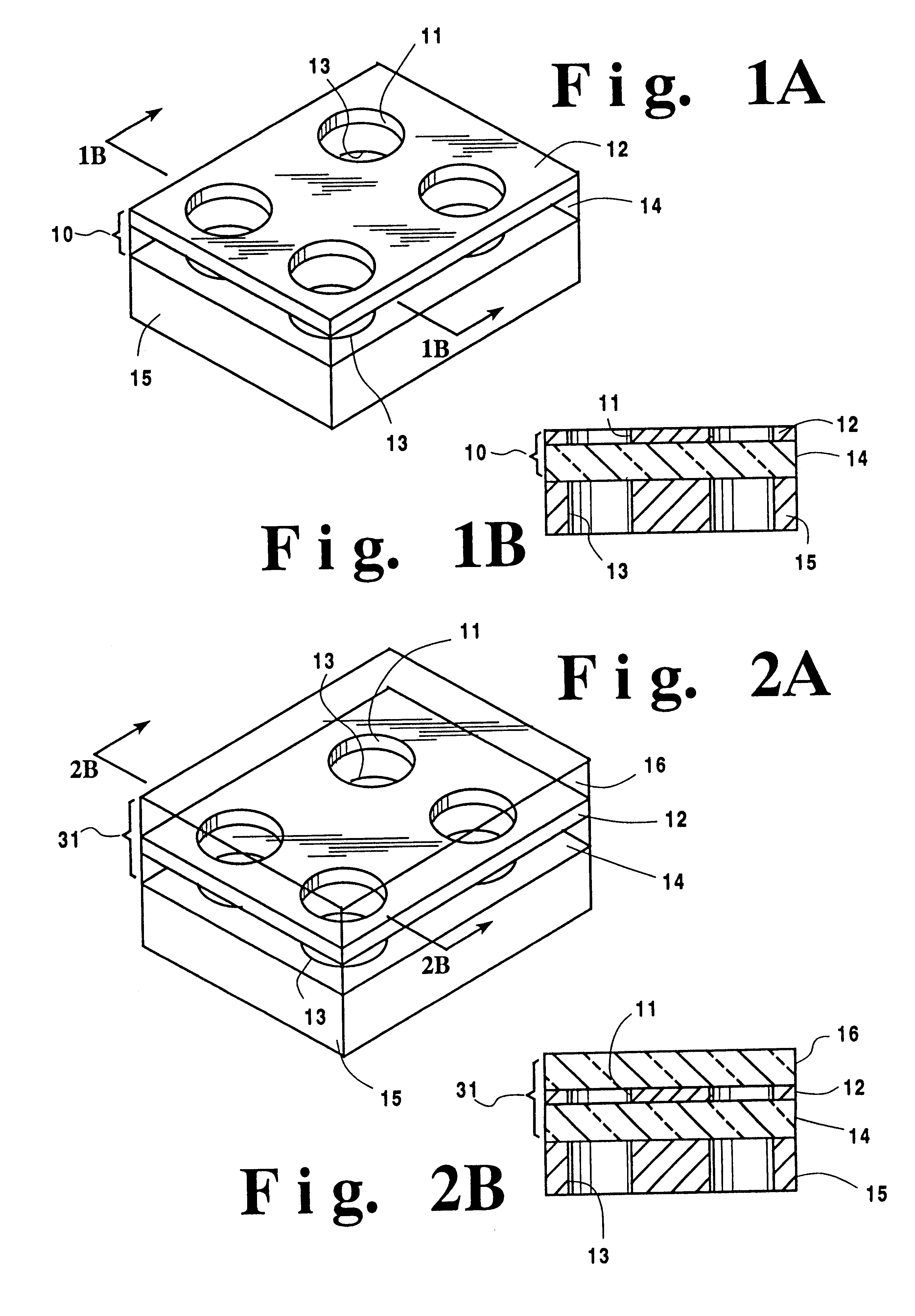
Referring to FIG. 1A, a via inspection mask is shown as 10. The mask 10 comprises a transparent substrate 14 having thereon an opaque pattern forming layer 12. Via inspection openings 11 in the opaque layer 12 are shown. These openings 11 are formed by etching of the opaque layer using a laser beam. The via inspection mask 10 is shown overlaying a substrate 15 containing corresponding via openings 13, which substrate is to be inspected for proper positioning of the vias and the size of the via openings on the substrate.

FIG. 1B is a cross-sectional side view of FIG. 1A along lines 1B. Via inspection mask 10 comprises a pattern forming layer 12 and a Mylar transparent substrate layer 14. Other transparent substrates such a...


PUM

PropertyMeasurementUnit
Transparencyaaaaaaaaaa
Fluorescenceaaaaaaaaaa

Abstract

Exposure masks and inspection masks for use in the electronics field may be made using laser beams wherein the mask comprises a substrate which is substantially unaffected by exposure to the laser beam and an opaque pattern forming layer on the substrate, which pattern forming layer absorbs the laser beam and is selectively etched when exposed to the laser beam. A preferred mask has an overcoat transparent layer. A cavity inspection mask is provided having a series of openings in the form of lines formed in the opaque pattern forming layer, the lines bounding the cavity walls, is the mask being used for determining if the cavity is centrally positioned on the substrate and/or that the cavity is of the desired size. Substrates containing identifying masks thereon which cannot be seen by the unaided eye for theft deterrence are also provided.

Description

1. Field of the InventionThe present invention relates to a method for making masks using lasers and in particular to exposure masks and punch inspection masks made using lasers.2. Description of Related ArtMasks are substrates having a defined pattern thereon and are used in a number of industrial applications in a wide variety of fields. The electronics field uses masks extensively to make printed circuit boards and integrated circuits and the different masks employed are generally categorized as exposure or photo masks, screening masks and inspection masks.For making integrated circuits (IC) on a silicon chip, the initial design and layout of an IC are carried out on a scale several hundred times larger than the final desired dimensions of the circuit pattern. The initial layout of an IC is normally done on a magnification scale in a range of 250:1 to 500:1 and the layout is a composite of different mask patterns corresponding to the different masking steps associated with the fa...

Claims


Application Information

Patent Timeline
IPC IPC(8): G03F9/00G03F1/00H05K3/00G03F1/68
CPCG03F1/68G03F9/00H05K3/0002
Inventor BALZ, JAMES GREGORYKAPFHAMMER, MARK WILLIAMLAPLANTE, MARK JOSEPHLONG, DAVID C.
Owner IBM CORP
Why Eureka
Try Eureka