Silicon-on-insulator (SOI) substrate and method of fabricating the same

a technology of silicon-on-insulator and substrate, which is applied in the direction of basic electric elements, electrical apparatus, semiconductor devices, etc., can solve the problems of affecting the characteristics of crystal defects, affecting the performance of the product, and affecting the quality of the produ

Inactive Publication Date: 2001-04-03
NEC CORP
View PDF10 Cites 190 Cited by
  • Summary
  • Abstract
  • Description
  • Claims
  • Application Information

AI Technical Summary

Problems solved by technology

However, the hydrogen ion separation process is accompanied with a problem that a resultant SOI active layer includes a lot of crystal defects therein.
Such a lot of crystal defects exert harmful influence on characteristics of a device to be formed on an SOI active layer including the crystal defects.
However, not only a method of reducing crystal defects, but also the reason why crystal defects are generated have not been found so far.
As a result, oxygen originally contained in a silicon substrate is precipitated, and the thus precipitated oxygen causes deformation in a silicon substrate, which in turn causes dislocation and / or rod-shaped crystal defects.
In conclusion, crystal defects in an SOI active layer fabricated by a hydrogen ion separation process are caused by oxygen originally contained in a silicon substrate.

Method used


Image

  • Silicon-on-insulator (SOI) substrate and method of fabricating the same
  • Silicon-on-insulator (SOI) substrate and method of fabricating the same
  • Silicon-on-insulator (SOI) substrate and method of fabricating the same

Examples


example 2

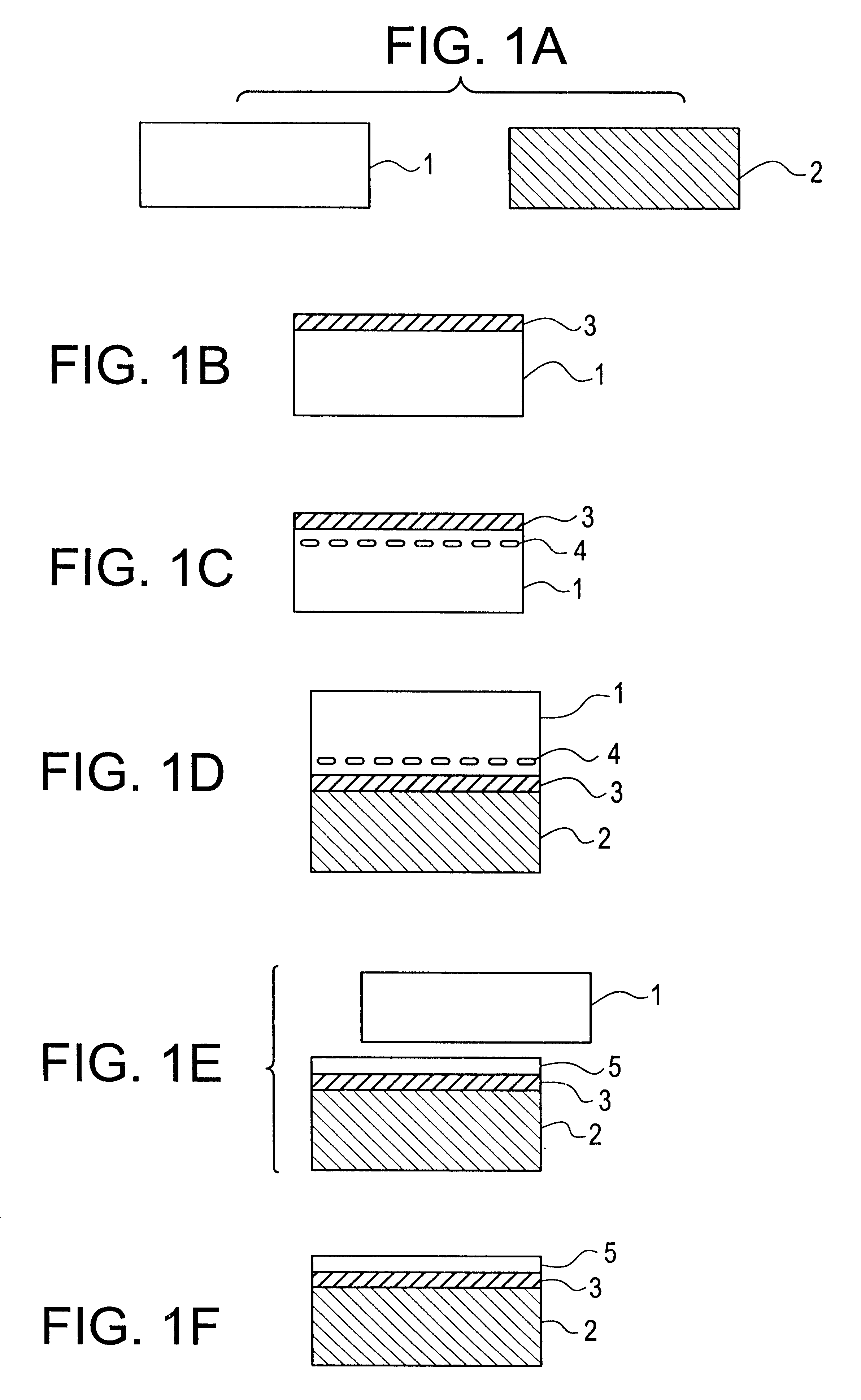
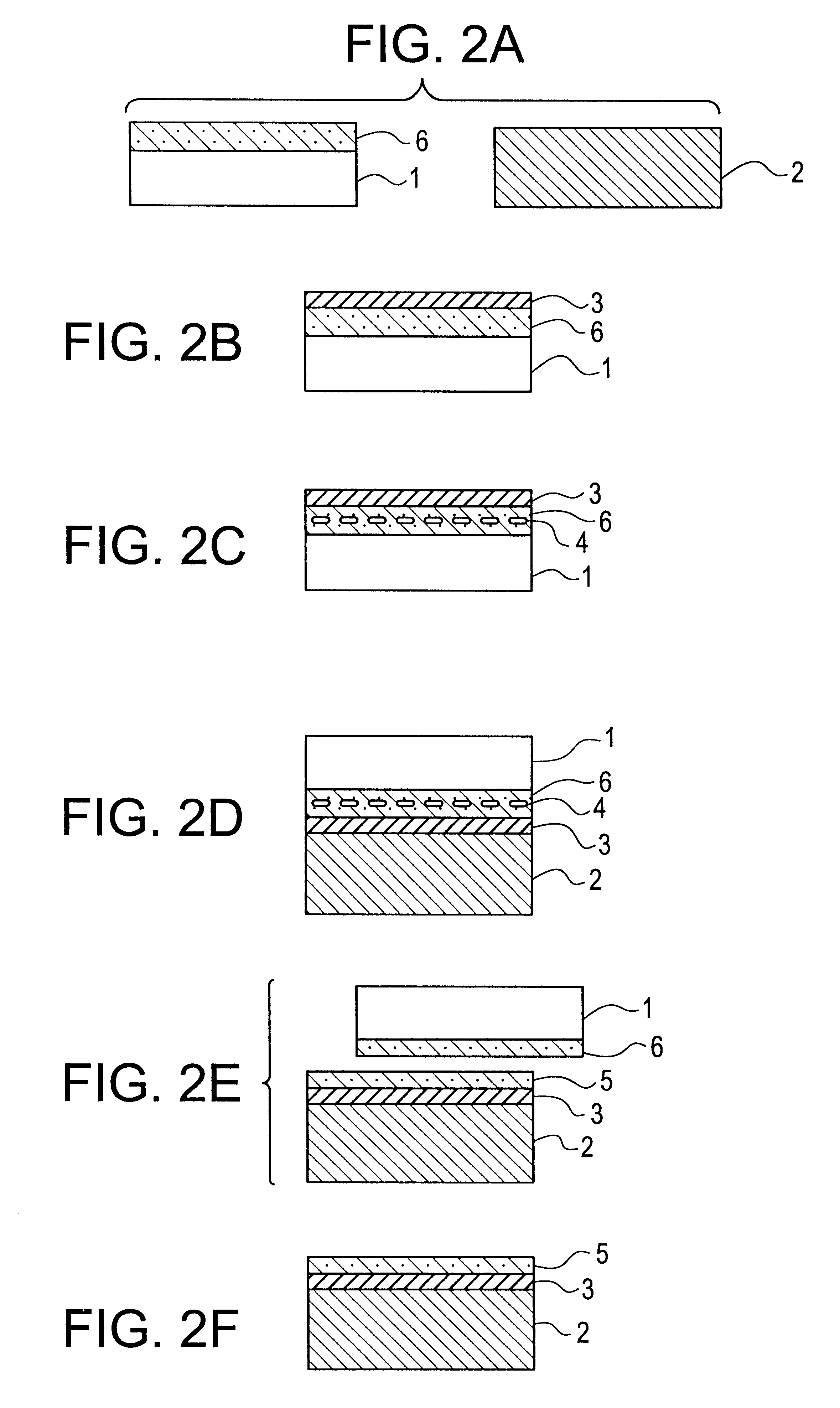
In the second example, an SOI substrate was fabricated by a hydrogen ion separation process, using a silicon wafer, as the silicon substrate 1, which was fabricated by MCZ process and contained oxygen at a concentration of 5.times.10.sup.17 / cm.sup.3.

In the second example, there were prepared six different support substrates A to F, as follows.

1. Support substrate A

The support substrate A has the same structure as the silicon substrate 1. That is, the support substrate A was a silicon wafer fabricated by MCZ process and containing oxygen at a concentration of 5.times.10.sup.17 / cm.sup.3.

2. Support substrate B

The support substrate B was fabricated by applying heat treatment at 1000 degrees centigrade in O.sub.2 atmosphere to the support substrate A for thermal oxidation. Accordingly, the support substrate B was formed at a surface thereof with a 0.1 .mu.m-thick oxide film.

3-6. Support substrates C-F

The support substrates C to F were the same as the support substrates C to F having be...

second embodiment

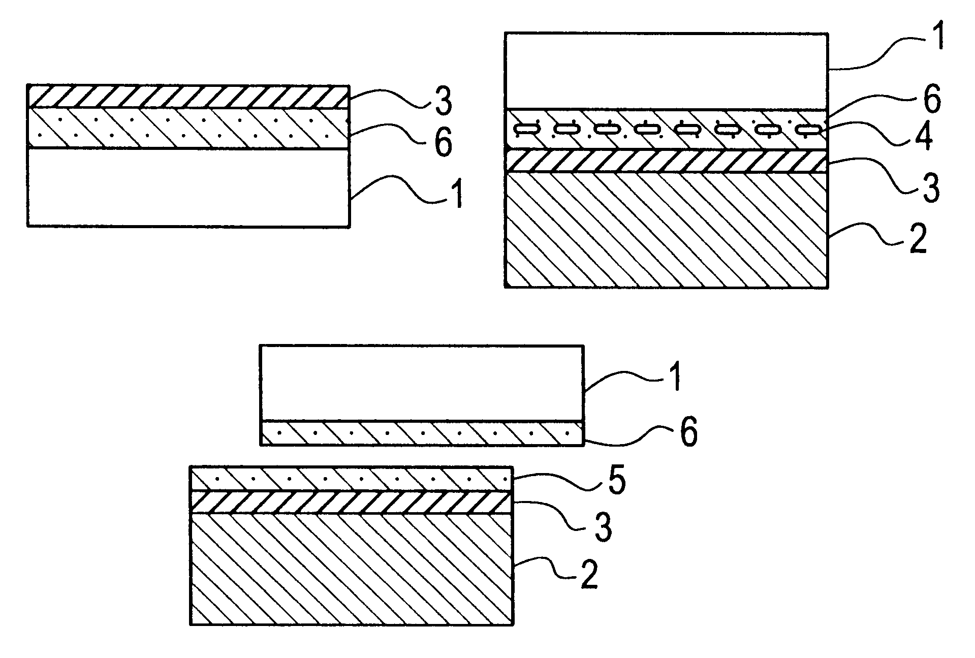
In the second embodiment, a silicon wafer containing oxygen at a relatively high concentration is used as a silicon substrate after a region thereof close to a surface, at which an SOI active layer is to be formed, has been treated so as to reduce an oxygen concentration in the region. In the above-mentioned first embodiment, a silicon wafer containing oxygen at a relatively low concentration was used as the silicon substrate 1. However, an SOI active layer on which a device is to be fabricated occupies merely a part of a surface of a silicon substrate. Accordingly, if a region at which an SOI active layer is to be fabricated is designed to contain oxygen at a relatively low concentration, other region of the silicon substrate is allowed to contain oxygen at a relatively high concentration.

A method of fabricating an SOI substrate in accordance with the second embodiment is explained hereinbelow with reference to FIGS. 2A to 2F.

In the second embodiment, a silicon substrate 1 is first...

example 3

In the third example, there was used a silicon wafer fabricated by CZ process and containing oxygen at a concentration of as the silicon substrate 1. The silicon substrate 1 was formed at a surface thereof with the region 6 containing oxygen at a relatively low concentration. Then, an SOI substrate was fabricated by a hydrogen ion separation process.

The region 6 was formed by applying heat treatment in argon atmosphere to the silicon substrate 1 to thereby form a denuded zone. The heat treatment was carried out at 1200 degrees centigrade at atmospheric pressure in 100%-argon atmosphere for 5 hours. The thus formed region 6 had a depth of 10 .mu.m and contained oxygen at a concentration of 8.times.10.sup.17 / cm.sup.3.

In the third example, there were prepared four different support substrates A to D, as follows.

1. Support substrate A

The support substrate A was a silicon wafer fabricated by CZ process and containing oxygen at a concentration of 2.times.10.sup.18 / cm.sup.3.

2. Support su...


PUM

PropertyMeasurementUnit
temperatureaaaaaaaaaa

Abstract

There is provided a method of fabricating a silicon-on-insulator substrate, including the steps of (a) forming a silicon substrate at a surface thereof with an oxygen-containing region containing oxygen at such a concentration that oxygen is not precipitated in the oxygen-containing region in later mentioned heat treatment, (b) forming a silicon oxide film at a surface of the silicon substrate, (c) implanting hydrogen ions into the silicon substrate through the silicon oxide film, (d) overlapping the silicon substrate and a support substrate each other so that the silicon oxide film makes contact with the support substrate, and (e) applying heat treatment to the thus overlapped silicon substrate and support substrate to thereby separate the silicon substrate into two pieces at a region into which the hydrogen ions have been implanted, one of the two pieces remaining on the silicon oxide film as a silicon-on-insulator active layer. The support substrate, the silicon oxide film located on the support substrate, and the silicon-on-insulator active layer formed on the silicon oxide film defines a silicon-on-insulator structure. The method makes it possible to significantly reduce crystal defect density in the silicon-on-insulator active layer, which ensures that a substrate made in accordance with the method can be used for fabricating electronic devices thereon.

Description

1. Field of the InventionThe invention relates to a method of fabricating a silicon-on-insulator substrate including an insulator and a silicon active layer formed on the insulator, and more particularly to such a method including a hydrogen ion separation process. The invention also relates to a silicon-on-insulator substrate suitable for a hydrogen ion separation process.2. Description of the Related ArtA silicon-on-insulator (hereinafter, referred to as "SOI") structure including a silicon active layer formed on an insulator is considered promising as a substrate to be used for next generation large scale integration (LSI). There have been suggested various methods of fabricating an SOI substrate.One of such various methods is a method having the steps of forming an oxide film on a surface of a silicon substrate, implanting hydrogen ions into the silicon substrate, overlapping the silicon substrate to a support substrate, and applying heat treatment to the thus overlapped silicon...

Claims


Application Information

Patent Timeline
Patent Type & Authority Patents(United States)
IPC IPC(8): H01L21/70H01L21/762H01L21/265H01L21/02H01L27/12
CPCH01L21/7624H01L21/76254Y10S257/914
Inventor OGURA, ATSUSHI
Owner NEC CORP
Why Eureka
Try Eureka