Method for integrated circuit power and electrical connections via through-wafer interconnects

a technology of electrical connection and through-wafer, which is applied in the direction of semiconductor devices, basic electric elements, electrical apparatus, etc., can solve the problems of reducing performance, reducing the practicability of ceramic substrate use, and increasing the cost of ceramic substrate manufactur

a technology of electrical connection and through-wafer, which is applied in the direction of semiconductor devices, basic electric elements, electrical apparatus, etc., can solve the problems of reducing performance, reducing the practicability of ceramic substrate use, and increasing the cost of ceramic substrate manufactur

US6221769B1Inactive Publication Date: 2001-04-24IBM CORP

Image

  • Method for integrated circuit power and electrical connections via through-wafer interconnects
  • Method for integrated circuit power and electrical connections via through-wafer interconnects
  • Method for integrated circuit power and electrical connections via through-wafer interconnects

Examples


Embodiment Construction

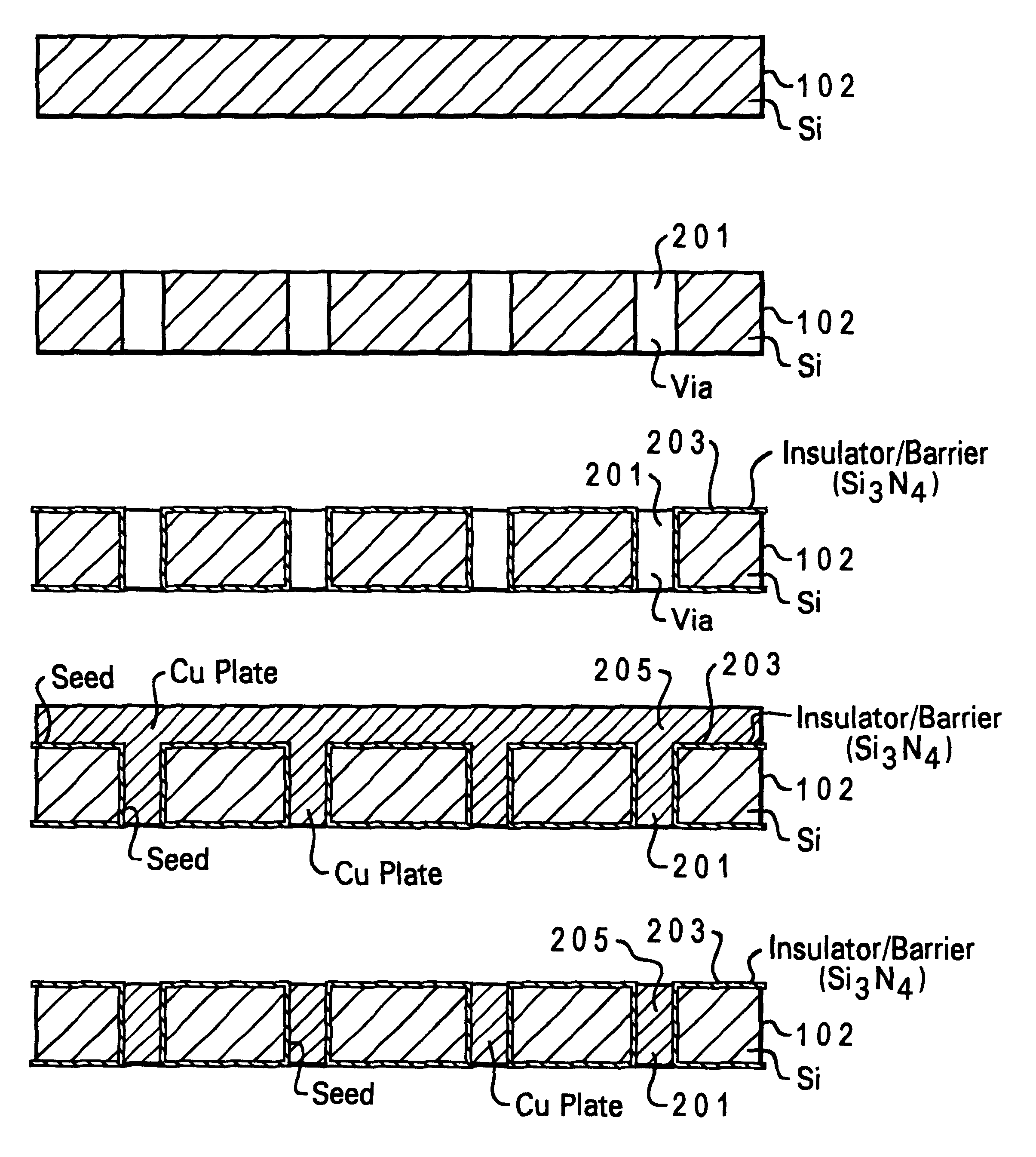
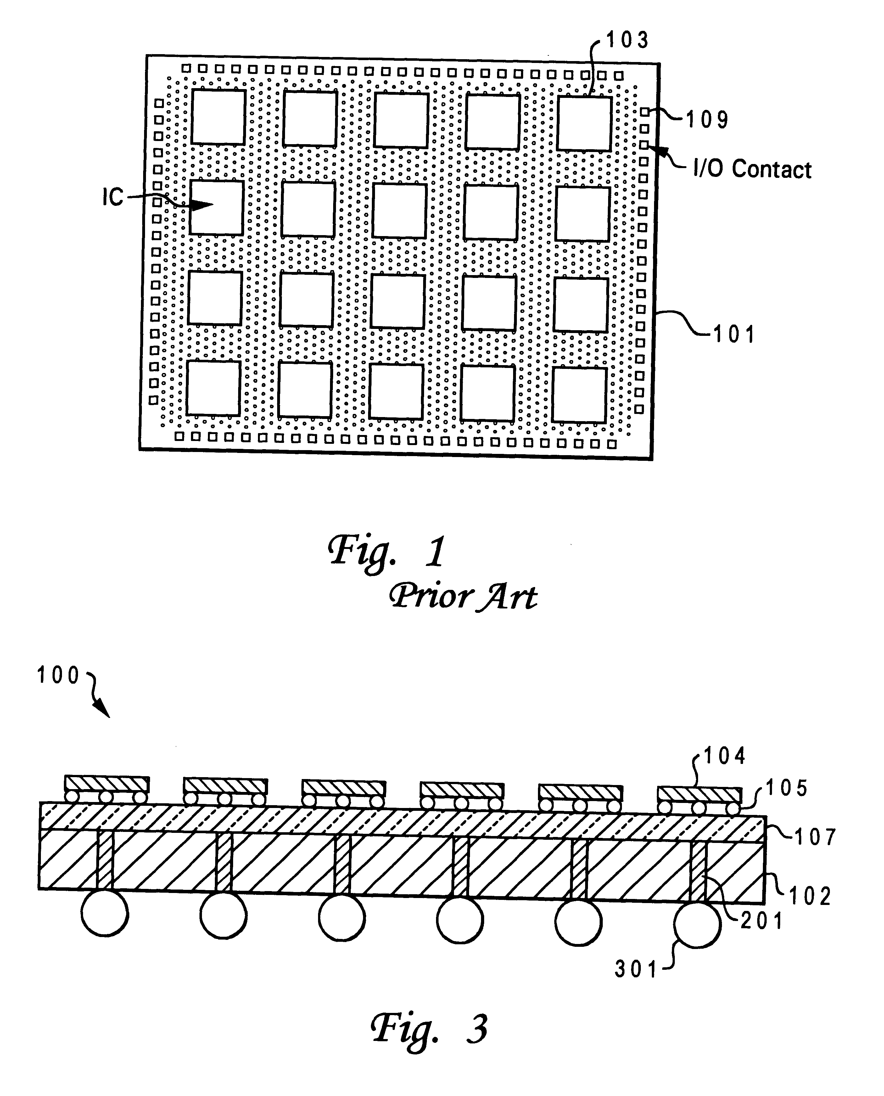
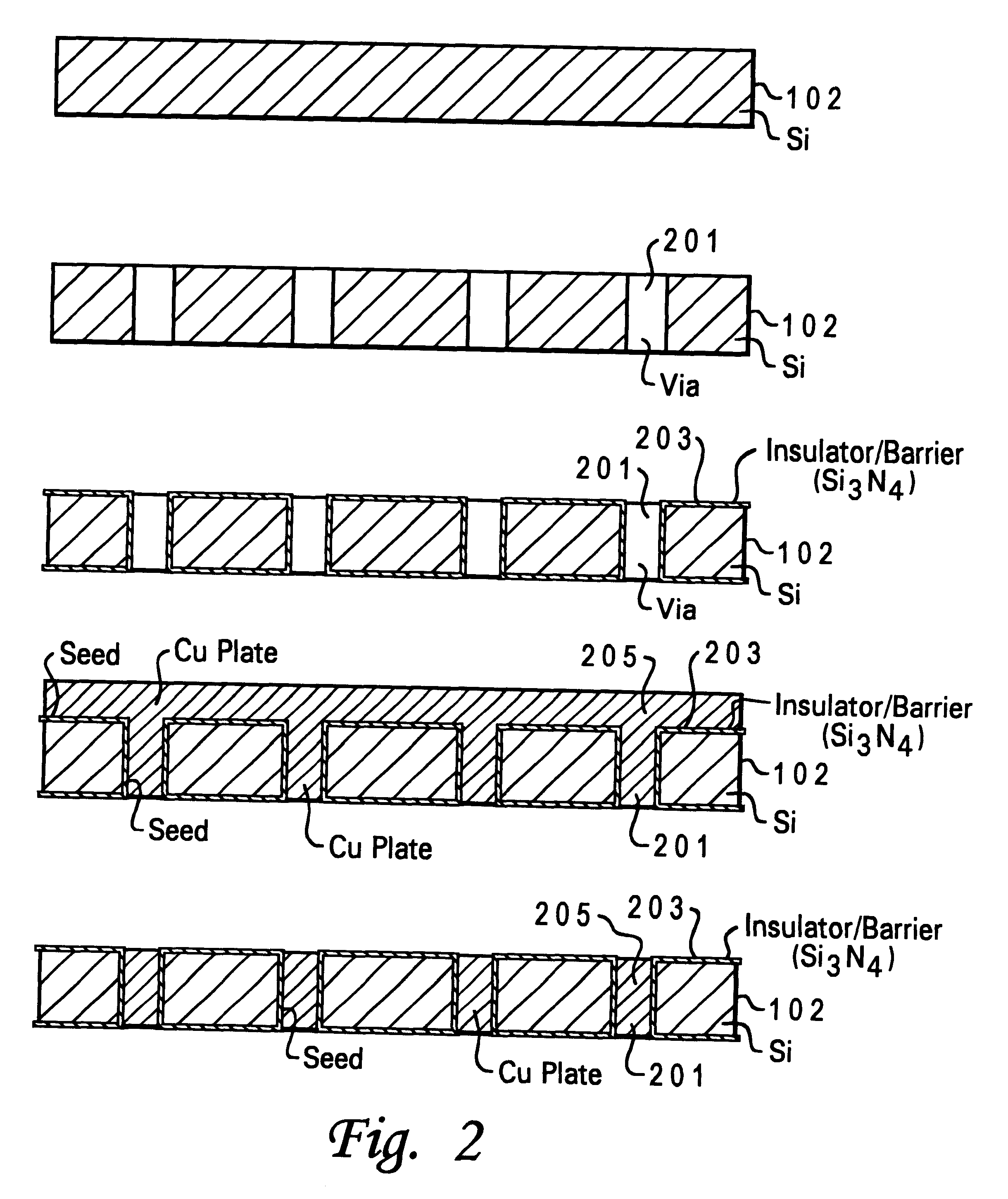
This invention describes a silicon package with vias formed through the wafer to achieve interconnection to other components. The invention further describes the methods utilized to create the vias in the silicon substrate. With reference now to the figures and in particular with reference to FIG. 2, the process of creating the silicon substrate of the preferred embodiment is depicted. In the preferred embodiment, the wafer is first patterned to allow for the vias to be made with particular sizes and placed in the desired locations and at predetermined separation distances to maximize the chip area.

A standard silicon substrate 102 is utilized in the invention. A plurality of vias 201 are created in silicon substrate 102. In the preferred embodiment, vias 201 are created in one of two ways. The first method utilizes mechanical drilling. The silicon wafer is first submerged in a liquid, preferably water and held down in place either mechanically or with a wax or other adhesive substan...


PUM


Abstract

A method for providing a through wafer connection to an integrated circuit silicon package. A hole is first created in the silicon package with an inner surface area extending from the bottom surface of the silicon package to the top surface of the silicon package. The hole is created by one of two methods. The first involves mechanical drilling with a diamond bit rotated at a high rate of speed. The second involves ultrasonically milling utilizing a slurry and steel fingers. The inner surface area of the hole is covered with an insulating material to insulate the conductive material which is later deposited and to serve as a diffusion barrier, then a seed material is placed in the hole. Finally, the hole is filled with a conductive material which is utilized to provide large power inputs or signaling connections to the integrated circuit chips.

Description

1. Technical FieldThe present invention relates in general to semiconductor devices and in particular to a method for creating a semiconductor chip package. Still more particularly, the present invention relates to a method for creating a semiconductor chip package having a silicon substrate with through-substrate vias for connecting to a power source and other electronic devices.2. Description of the Related ArtDue to an ever-increasing demand for performance and miniaturization, semiconductor manufacturers are continually driven to produce smaller and more efficient semiconductor devices. In order to reduce the size of semiconductor device packages, manufacturers have developed single and multi-chip modules (SCMs and MCMs) that efficiently house semiconductor chips having a large number of connections. A countervailing consideration in semiconductor device development is a desire to provide additional signal connections, and power connections for large power input to the semicondu...

Claims


Application Information

Patent Timeline
24 Apr 2001
Publication
US6221769B1
IPC
H01L21/48; H01L21/02; H01L21/768; H01L21/70
CPC
H01L21/486; H01L21/76898; H01L2224/16; H01L2924/01078; H01L2924/15312; H01L2924/01322; H01L2924/10253; H01L2924/00
Inventors
DHONG, SANG HOO; NOWKA, KEVIN JOHN