Method and apparatus for sequentially etching a wafer using anisotropic and isotropic etching

a technology of anisotropic and isotropic etching and sequential etching, which is applied in the direction of electrical apparatus, decorative surface effects, decorative arts, etc., can solve the problems of large number of steps, large risk of device damage and contamination, and large number of process steps to achieve the desired structure in the film stack. achieve the effect of facilitating in situ etching

Inactive Publication Date: 2001-04-24
APPLIED MATERIALS INC
View PDF10 Cites 30 Cited by
  • Summary
  • Abstract
  • Description
  • Claims
  • Application Information

AI Technical Summary

Problems solved by technology

Although the foregoing process yields a structure that is effectively used in a DRAM device, the number of process steps, and the number of chambers (both etch and deposition) required to produce the desired structure in the film stack is large.
With such a large number of steps, and associated chambers required to execute those steps, the risk of device damage and contamination is correspondingly large as well.
Additionally, the large number of steps places a burden on system throughput.
Since prior art reactors are typically not capable of the selectivity needed to etch the underlying polysilicon without damaging nitride and oxide layers exposed in the film stack, a separate tool is typically used for the polysilicon etching step that follows in some specific process sequences.
The need for switching chambers to etch the underlying polysilicon after the oxide etch increases the risk of damage to the film stack by exposing the wafer to additional environments and excessive handling.

Method used


Image

  • Method and apparatus for sequentially etching a wafer using anisotropic and isotropic etching
  • Method and apparatus for sequentially etching a wafer using anisotropic and isotropic etching
  • Method and apparatus for sequentially etching a wafer using anisotropic and isotropic etching

Examples


Embodiment Construction

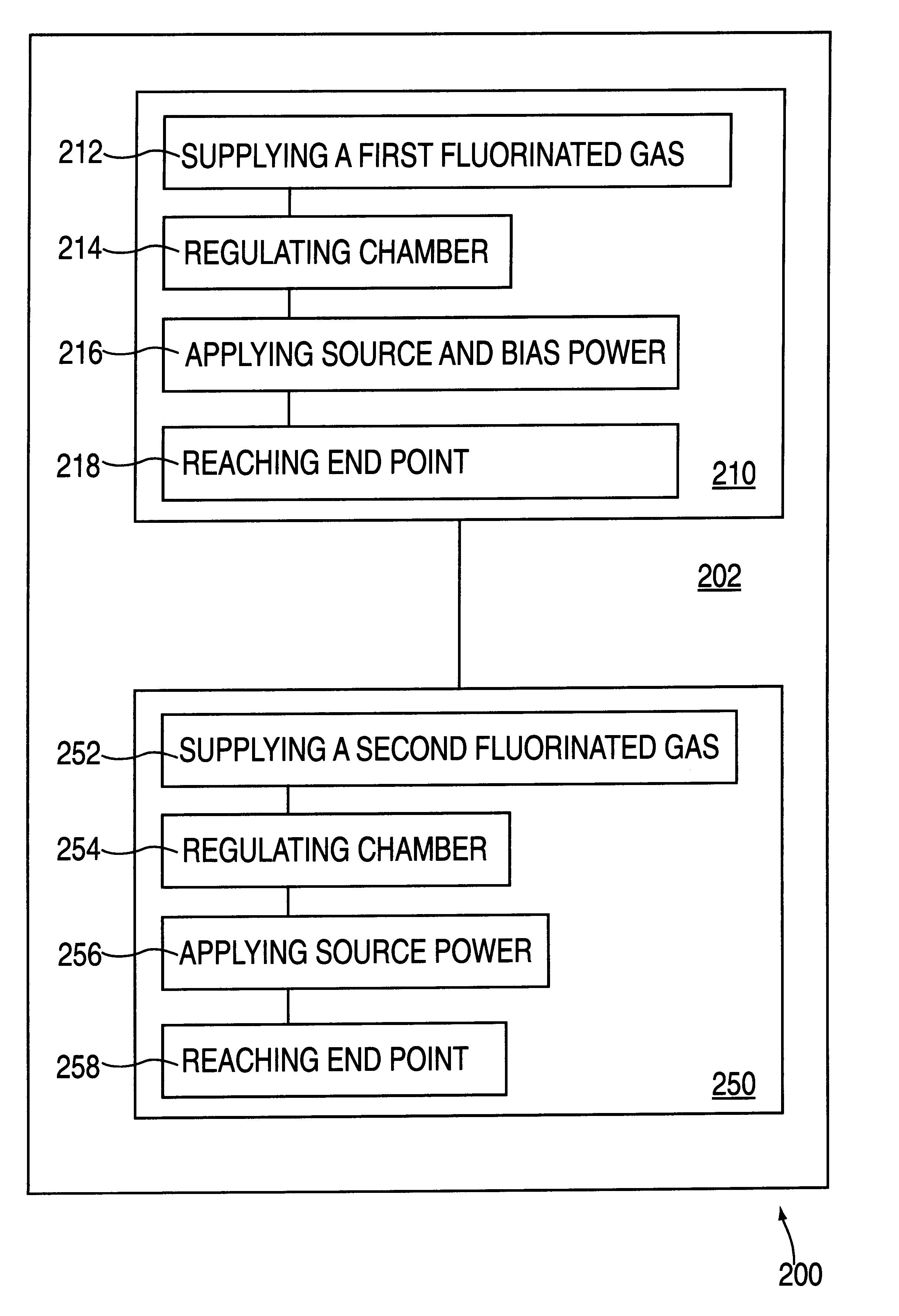
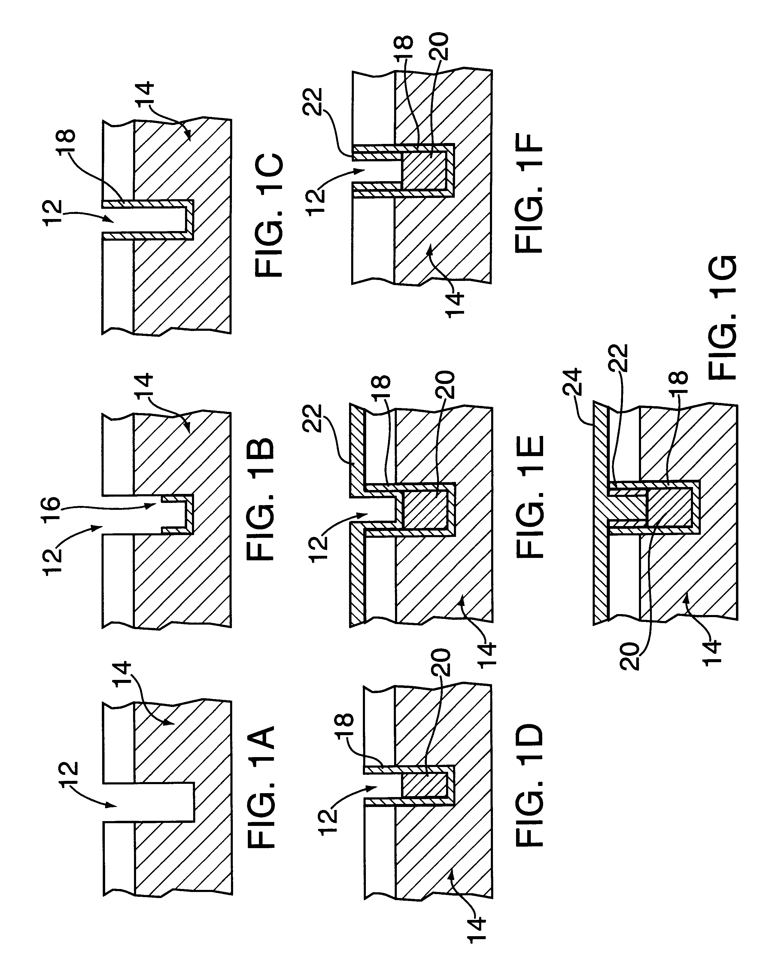
An embodiment of the present invention is a method of etching a substrate comprising a dielectric layer overlying a polysilicon layer. The embodiment of the present invention etches the dielectric to expose a polysilicon material that is subsequently etched. Both the dielectric and polysilicon etch occur sequentially within the same chamber of an etching system, i.e., in situ. The etch process of the present invention can be reduced to practice in a number of etching systems capable of etching both dielectric and polysilicon materials where the selectivity of the dielectric to the polysilicon can be varied. One such chamber is a Decoupled Plasma Source (DPS) Centura etch system available from Applied Materials, Inc., of Santa Clara, Calif.

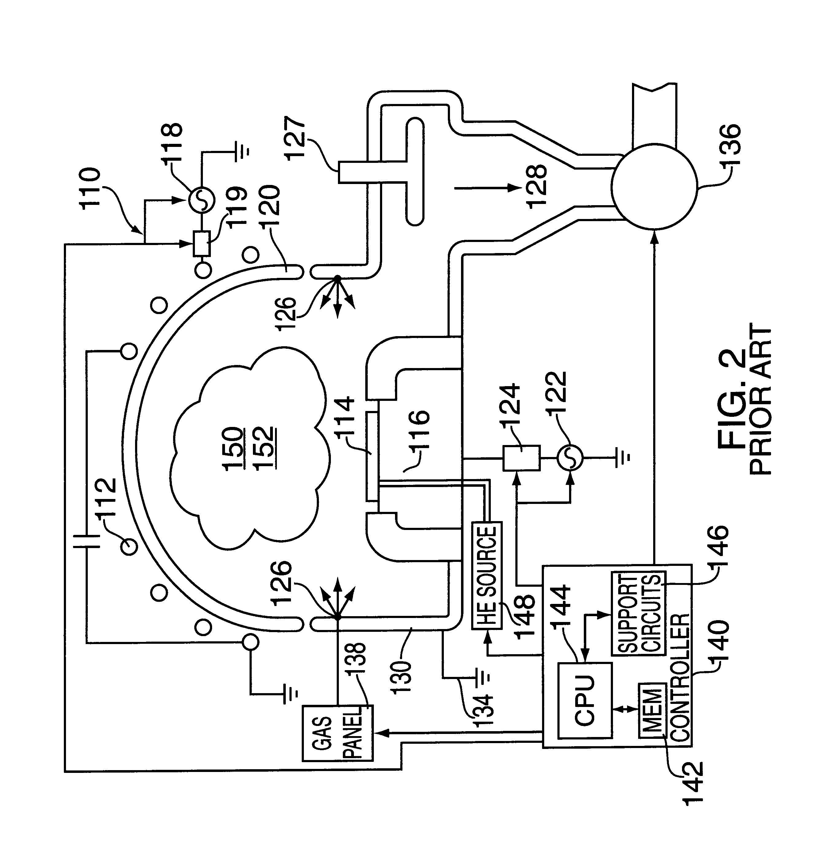
FIG. 2 depicts a schematic diagram of the DPS etch process chamber 110, that comprises at least one inductive coil antenna segment 112, positioned exterior to a dielectric, dome-shaped ceiling 120 (referred hereinafter as the dome 120). The antenna...


PUM

PropertyMeasurementUnit
poweraaaaaaaaaa
bias poweraaaaaaaaaa
inductive source poweraaaaaaaaaa

Abstract

An apparatus and method for in-situ etching of a substrate comprising both a polysilicon layer and an overlying dielectric layer. An embodiment of the method comprises an anisotropic etch of the dielectric layer in a chamber using a first fluorinated gas (such as CF4, NF3, SF6, and the like) as an etch gas to expose at least a portion of underlying polysilicon layer. Following the anisotropic etch and without removing the substrate from the chamber, i.e., in situ, an isotropic etch is preformed on the underlying polysilicon layer using a second fluorinated gas (such as CF4, NF3, SF6, and the like) as an etch gas.

Description

BACKGROUND OF THE DISCLOSURE1. Field of InventionThe present invention relates generally to a method and apparatus for dry etching semiconductor wafers. More specifically, the invention relates to a method and concomitant apparatus for anisotropically etching a dielectric layer followed by in situ isotropic etching of a polysilicon layer.2. Background of InventionTrenches formed in semiconductor substrates have many uses in producing integrated circuits including isolation, capacitor formation, transistor formation, and so forth. One important use of trenches is in the formation of a trench capacitor as a storage node for a dynamic random access memory (DRAM) device. Trench capacitors are desirable because they occupy a relatively small area, while having large electrode surface area due to the depth of the trench used to form the capacitor.FIGS. 1A through 1G collectively depict a portion of a conventional process of manufacturing the DRAM structure. In a first process chamber, a t...

Claims


Application Information

Patent Timeline
Patent Type & Authority Patents(United States)
IPC IPC(8): H01L21/02H01L21/3213H01L21/311
CPCH01L21/31116H01L21/32137
Inventor SCHMIDT, URSULASCHOENLEBER, WALTERSCHMIDT, MICHAEL
Owner APPLIED MATERIALS INC
Why Eureka
Try Eureka