

Poly routing for chip interconnects with minimal impact on chip performance
a technology of interconnects and poly routing, which is applied in the field of microelectronic integrated circuits, can solve the problems of limited prior art algorithms, physical design is not practicable without the aid of computers, and the layout of the entire circuit cannot be handled
- Summary
- Abstract
- Description
- Claims
- Application Information
AI Technical Summary
Problems solved by technology
Method used
Image

Examples
Embodiment Construction
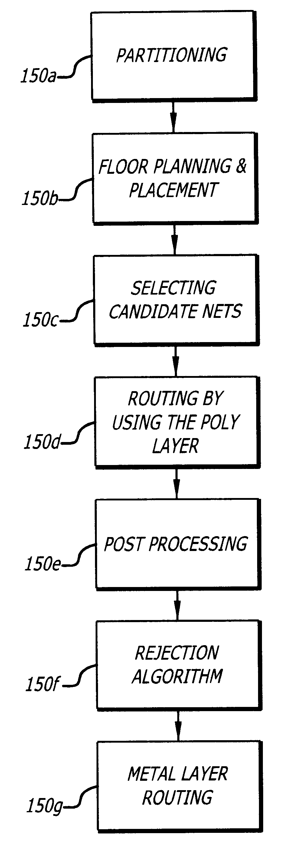
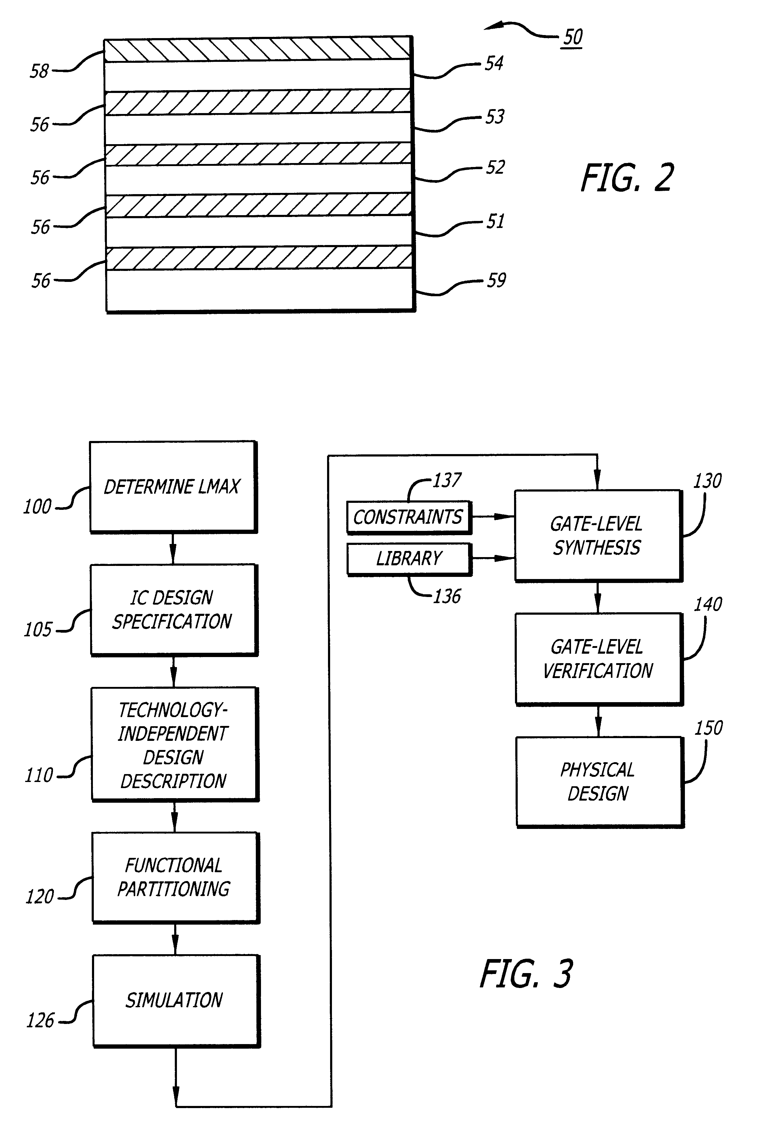
FIG. 3 illustrates a flow diagram for providing an overview of ASIC chip design according to preferred embodiments of the present invention. It should be understood that the description contained herein are in terms of a suite of software "blocks" used in a CAD system that can be run on any suitable computer system.
It should be noted that the underlying database used by the CAD system in accordance with preferred embodiments of the present invention needs to include the modeling of the poly layer in the database. For example, a CAD system, which just uses metal layers for routing, may not be including the modeling of the poly layer, poly ports and wires internal to the cells in the abstraction of the standard cells contained in the standard cell library. Basically, for a matter of convenience, the abstraction of the standards cells contained in the standard cell library may omit poly layer information including a via layer connection to the metal-1 layer because such information is ...
PUM
 Abstract
Description
Claims
Application Information