Method for crystallizing amorphous layer

a technology of amorphous layer and crystallization method, which is applied in the direction of crystal growth process, polycrystalline material growth, gel state, etc., can solve the problems of inapplicability to glass substrates, and inconvenient crystallization by laser crystallization

Inactive Publication Date: 2001-06-05
LG DISPLAY CO LTD
View PDF4 Cites 52 Cited by
  • Summary
  • Abstract
  • Description
  • Claims
  • Application Information

AI Technical Summary

Problems solved by technology

Laser crystallization, however, is not useful for the purpose of formation of polysilicon layer on a substrate which is large in area, because the polysilicon layer in this case is not formed uniformly and costs a great deal due to the use of expensive equipment for which the yields are low.
However, it is inapplicable to a glass substrate since the layer crystallizes at relatively high temperatures only after a long time, plus the yields are low.
However, an example of the problem with such a metal-induced crystallization of amorphous silicon lies in the change of inherent properties of the silicon layer that results from contaminant metals entering the polysilicon layer.
Furthermore, heat treatment takes a long time i.e. 10 hours or more, and the growth temperature is relatively high.
An increase in the amount of metal substantially increases the efficiency of metal-induced crystallization, but also raises the problem of metal-contamination.

Method used


Image

  • Method for crystallizing amorphous layer
  • Method for crystallizing amorphous layer
  • Method for crystallizing amorphous layer

Examples


Embodiment Construction

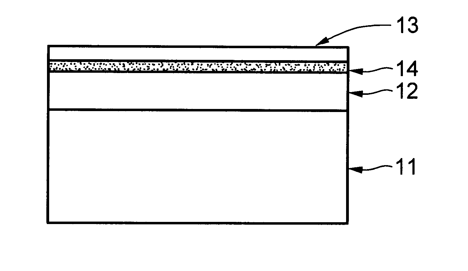
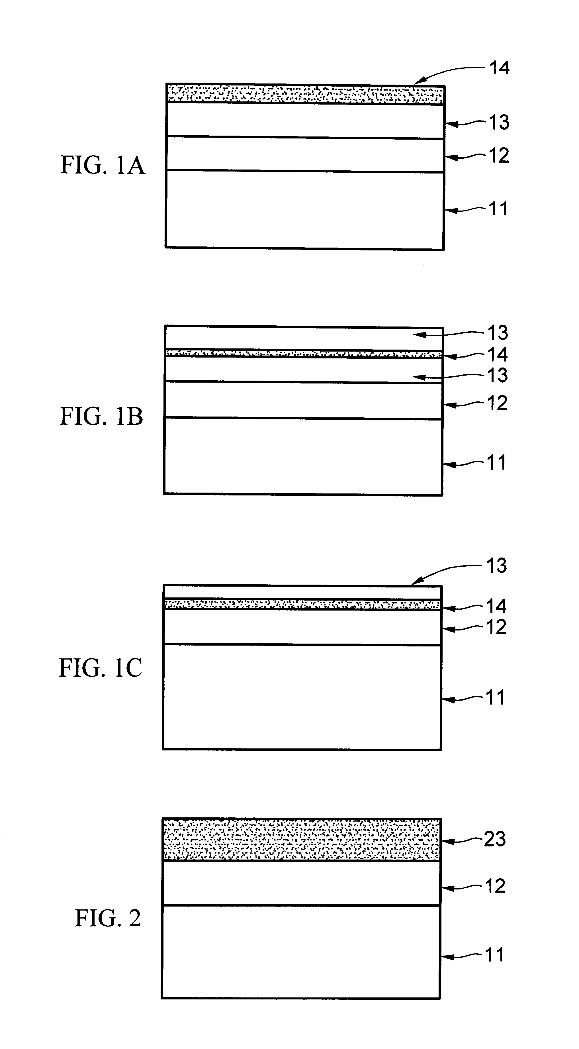
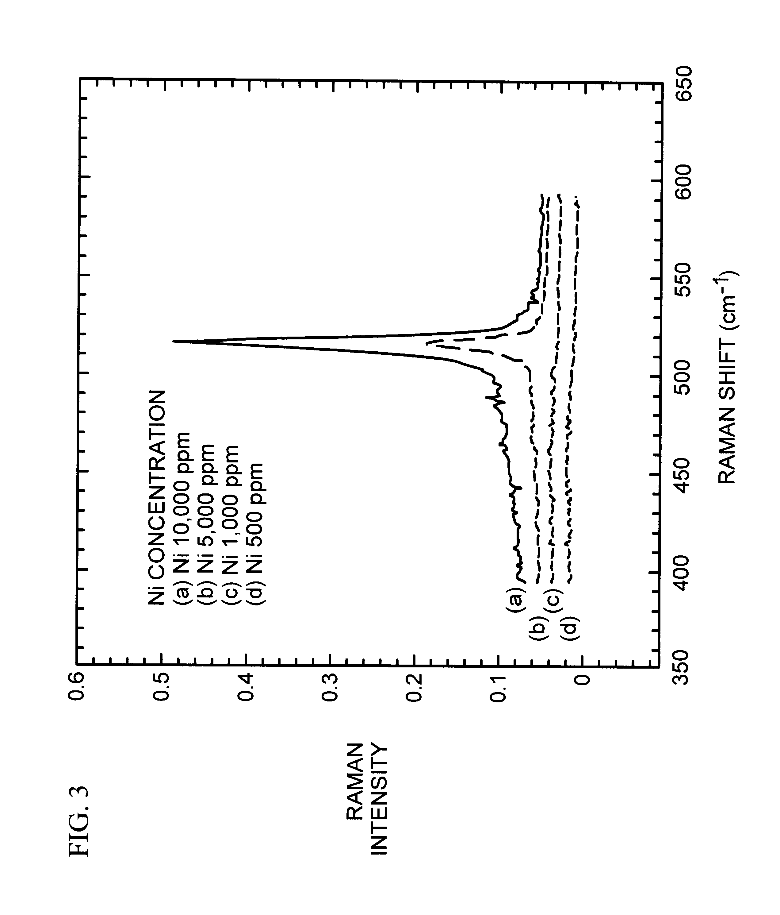
FIGS. 1A-1C illustrate three examples of crystallization of amorphous silicon making use of a nickel solution in accordance with a first preferred embodiment of the present invention. The nickel solution is prepared by dissolving nickel in acid solution, such as nitric solution or hydrochloric solution. In cross section of the respective substrates in the following embodiments, amorphous silicon layer is formed in the 100 to 10,000 .ANG. range of thickness and nickel film is around 0.1 to 100 .ANG. thick.

As shown in FIG. 1A, amorphous silicon layer 13 is first formed on an insulating substrate 11 and then coated with a nickel solution, forming a nickel film 14. The insulating substrate 11 is preferably normally made of quartz, glass or an oxide layer. A buffer layer 12 may be interposed between the insulating substrate 11 and the amorphous silicon layer 13 in order to prevent impurities of the insulating substrate 11 from entering the amorphous silicon layer 13 during the crystalliz...


PUM

PropertyMeasurementUnit
thicknessaaaaaaaaaa
thickaaaaaaaaaa
temperaturesaaaaaaaaaa

Abstract

A method for crystallizing an amorphous layer into a polycrystalline layer. The method uses a substrate under the amorphous layer and a nickel film on the amorphous layer, which are subjected to a heat treatment. The nickel film is formed by a coating step that uses a nickel-containing solution. Alternatively, a nickel and gold, or a nickel and palladium, solution can be used. The method eliminates contamination with metal in the polycrystalline silicon layer and reduces its growth temperature.

Description

1. Field of the InventionThe present invention generally relates to a method for crystallizing amorphous layer. More particularly, the present invention relates to a method for crystallizing amorphous layer wherein the amorphous layer is coated with a nickel-containing solution and heated afterwards.2. Discussion of Related ArtPolysilicon layer has been employed for the active layer of a thin film transistor in semiconductor devices, notably liquid crystal display devices. This is because the polysilicon layer has a high carrier mobility relative to amorphous silicon layer. Such polysilicon is normally grown at high temperatures. However, there have been recently developed techniques for fabrication of polysilicon thin film transistors at low temperatures.This low-temperature polysilicon involves some advantages in that it can be processed at low temperatures, can form large areas and can perform comparably to high formation-temperature polysilicon.Many techniques are known for crys...

Claims


Application Information

Patent Timeline
Patent Type & Authority Patents(United States)
IPC IPC(8): C30B1/02C30B1/00
CPCC30B1/023C30B29/06
Inventor JANG, JINYOON, SOO-YOUNGOH, JAE-YOUNG
Owner LG DISPLAY CO LTD
Why Eureka
Try Eureka