Method to selectively heat semiconductor wafers

a technology of selective heating and semiconductor wafers, applied in semiconductor devices, semiconductor/solid-state device details, electrical devices, etc., can solve the problems of inability to selectively heat wafers, easy contamination of wafers,

Inactive Publication Date: 2001-06-12
LUCENT TECH INC +1
View PDF8 Cites 95 Cited by
  • Summary
  • Abstract
  • Description
  • Claims
  • Application Information

AI Technical Summary

Problems solved by technology

A problem with using a furnace is that the wafers are susceptible to contamination from the hot processing in the core 2 on which deposited films may accumulate and flake off or through which impurities may diffuse and contaminate wafers 4.
This method does not address selective application of film on the wafer to alter the temperature.
This method is used for reducing the effects of semiconductor deformities and does not address temperature differences in heating the wafer.
However, if the film is too thick, it may have a reverse effect by decreasing the temperature due to the low thermal conductivity of dielectric film.

Method used


Image

  • Method to selectively heat semiconductor wafers
  • Method to selectively heat semiconductor wafers
  • Method to selectively heat semiconductor wafers

Examples


Embodiment Construction

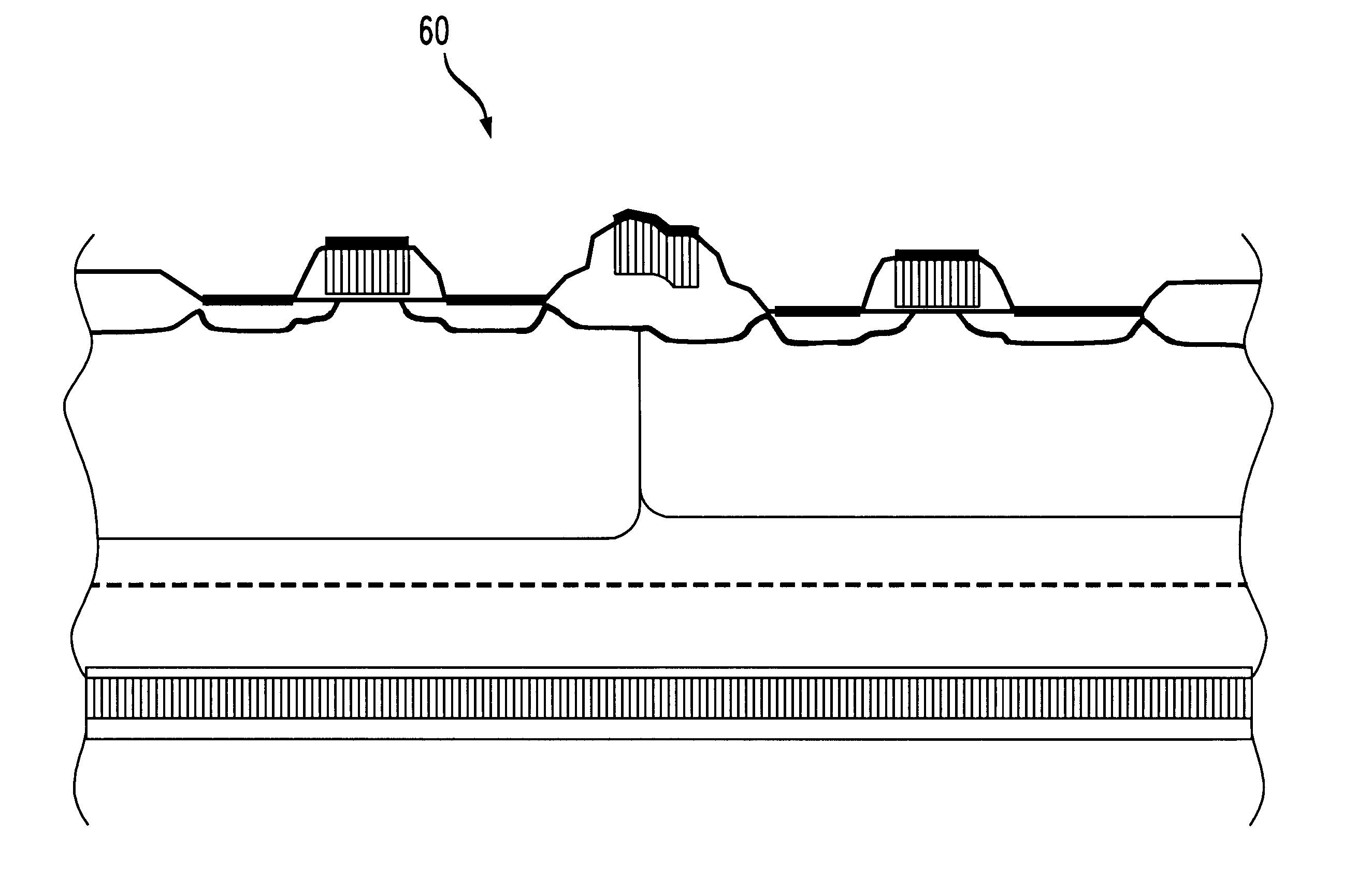
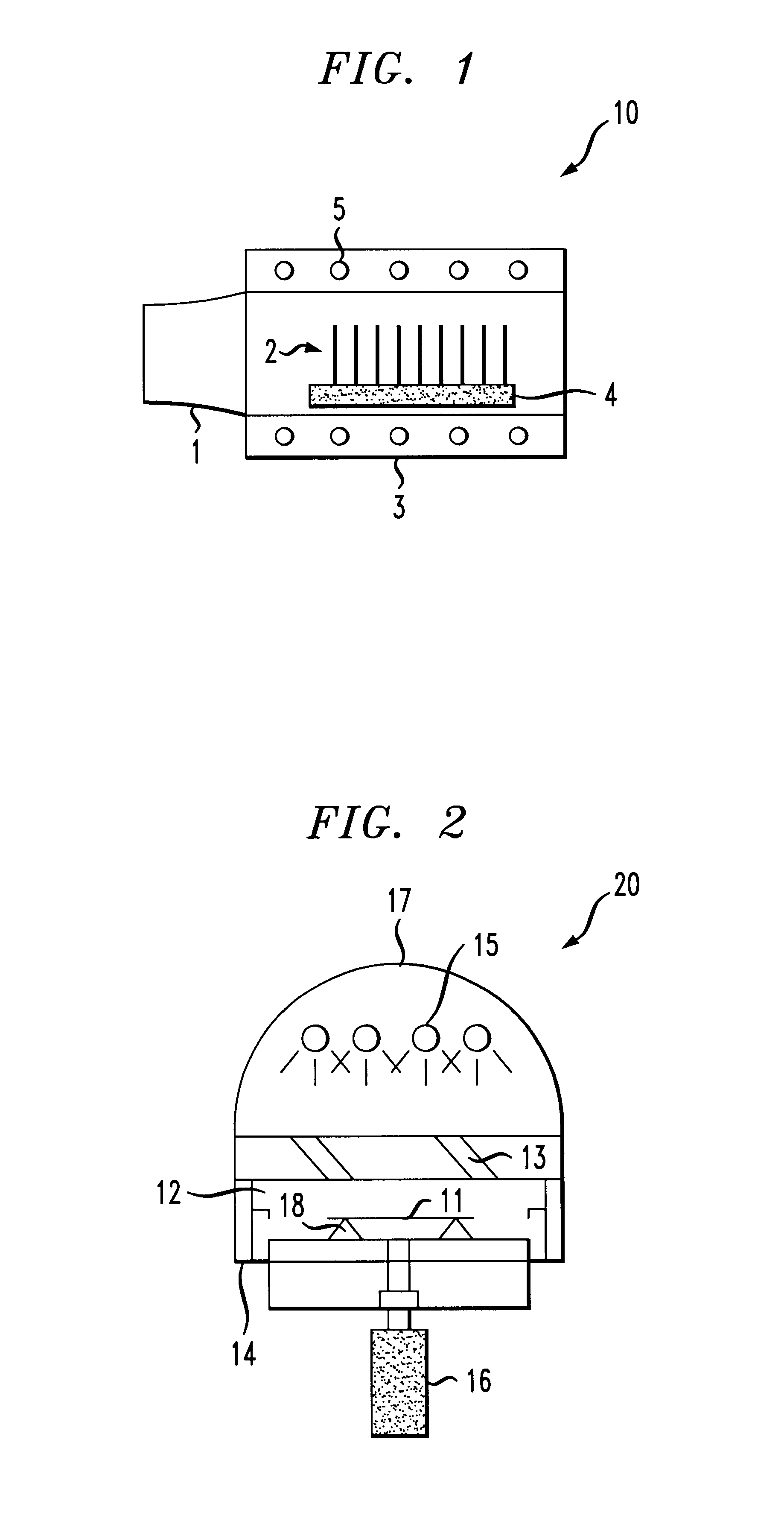
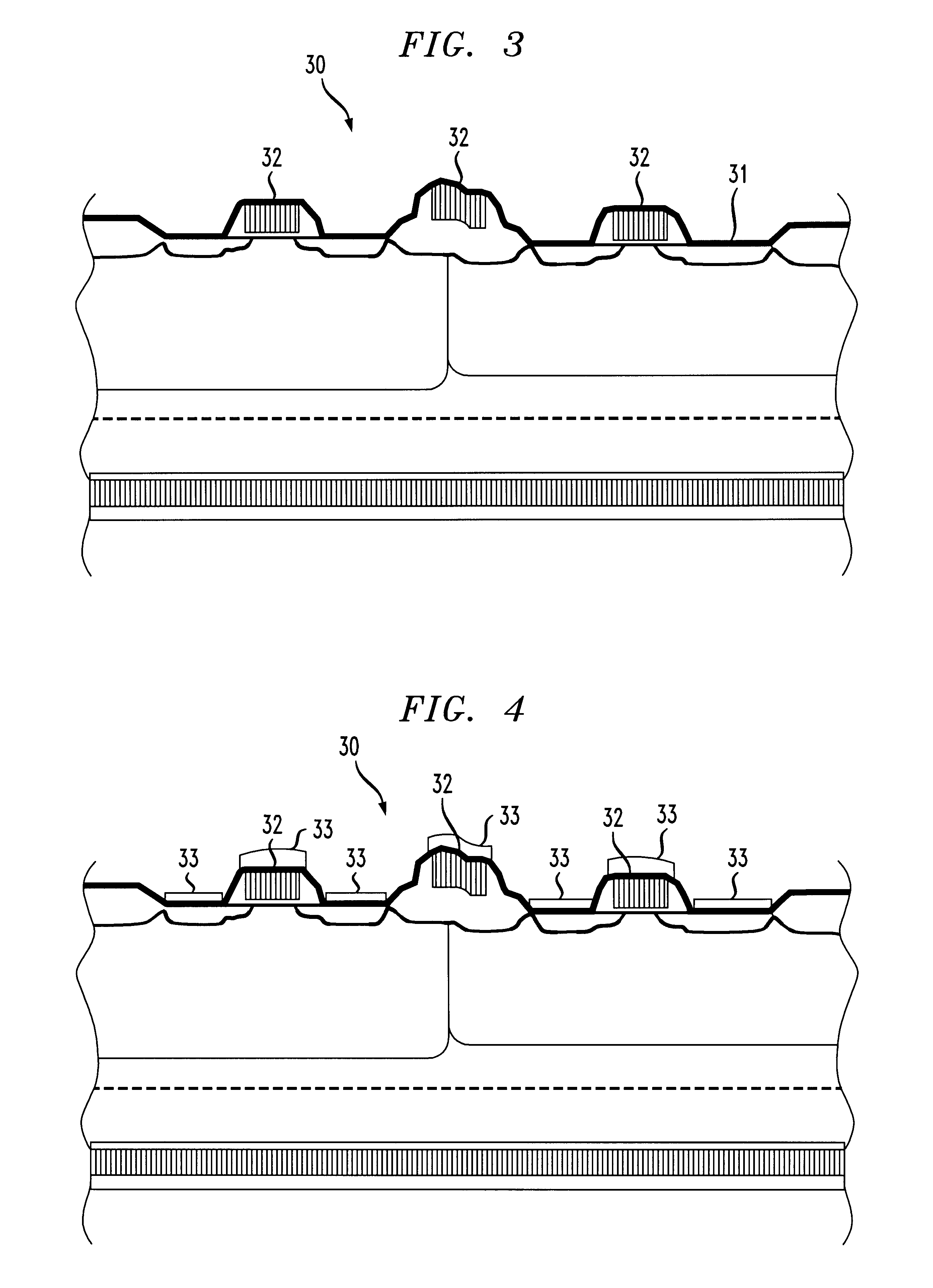
In one experiment, the reaction of Ti and Si forming TiSi.sub.2, or self-aligning titanium silicide, was examined. A wafer having exposed surfaces of Si was provided. After deposition of titanium, which is a metal of low emissivity, the titanium was coated with an oxide film of 1000 .ANG.to improve the heat flow. The silicide was selectively formed by a rapid thermal process, in this case, a rapid thermal annealer having a heating lamp and a processing chamber, at a reaction temperature of 650.degree. C. A pyrometer of a closed loop temperature control system sensed an average wafer temperature to control the heating lamp. In this process, the temperature must be comparatively high to achieve complete silicidation on silicon, but as low as possible to avoid any reaction with SiO.sub.2. The amount of TiSi.sub.2 formed with the presence ofthe oxide film indicated a temperature differential of 20.degree. C. which is consistent with the prior set of calculations. Typically, this method ...


PUM

PropertyMeasurementUnit
temperatureaaaaaaaaaa
emissivityaaaaaaaaaa

Abstract

A method for manufacturing integrated circuits; particularly, a method to alter heat flow on a localized basis, when heating wafers to elevated temperatures, to achieve different processing temperatures by altering the material properties, such as emissivity, absorptivity and reflectivity, of a portion of a surface by the application of thin films of various materials.

Description

1. Field of the InventionThis invention relates to a method of manufacturing semiconductor integrated circuit interconnect structures. The invention relates more particularly to a method to alter heat flow on a localized basis when heating wafers to elevated temperatures to achieve different processing temperatures by altering the material properties, such as emissivity, absorptivity, and reflectivity, of a portion of a surface by the application of thin films of specified materials.2. Background of the InventionA. Field of the InventionThis invention relates to a method for fabricating semiconductor integrated circuit devices, specifically with a method for fabricating semiconductor integrated circuit devices enabling the creation of temperature differentials.B. Description of the Related Art.Semiconductor integrated circuit devices typically comprise silicon and multiple layers of vertically stacked metal interconnect layers with dielectric materials disposed between them. The fab...

Claims


Application Information

Patent Timeline
Patent Type & Authority Patents(United States)
IPC IPC(8): H01L21/02H01L21/336H01L21/324H01L21/28H01L21/26H01L21/314H01L21/3205H01L23/52
CPCH01L21/324H01L29/665
Inventor PEARCE, CHARLES WALTERBILLIG, MICHAEL STEVEN
Owner LUCENT TECH INC
Why Eureka
Try Eureka