
Metal-insulator-metal capacitor for copper damascene process and method of forming the same

a technology of metal-insulator and capacitor, which is applied in the direction of capacitors, semiconductor devices, semiconductor/solid-state device details, etc., can solve the problems of changing the capacitance, p-p capacitors are becoming less popular, and p-p capacitors suffer from carrier depletion

Inactive Publication Date: 2001-07-10
IBM CORP
View PDF4 Cites 121 Cited by
  • Summary
  • Abstract
  • Description
  • Claims
  • Application Information

AI Technical Summary

Problems solved by technology

However, P-P capacitors are becoming less popular because they present a number of problems when used with complementary metal oxide semiconductor (CMOS) technologies.
However, P-P capacitors suffer from carrier depletion which changes the capacitance as surface voltage across the P-P capacitor changes.
Therefore, P-P capacitors do not maintain the linearity required in today's sophisticated analog circuits.
Further, P-P capacitors often trap charges within the insulator during their use.
However, MIM capacitors also present manufacturing problems.
More specifically, conventional MIM capacitors with an SiO.sub.2 insulator cannot be used over copper damascene metal wiring because copper diffuses through the capacitor structure and creates leakage.
In other words, the copper is not a good electrode in the conventional capacitor structures.
This is a substantial disadvantage because copper damascene wiring is becoming more popular in CMOS technologies because copper is less expensive and has better conductivity and electromigration resistance when compared to aluminum wiring.

Method used


Image

  • Metal-insulator-metal capacitor for copper damascene process and method of forming the same
  • Metal-insulator-metal capacitor for copper damascene process and method of forming the same
  • Metal-insulator-metal capacitor for copper damascene process and method of forming the same

Examples


Embodiment Construction

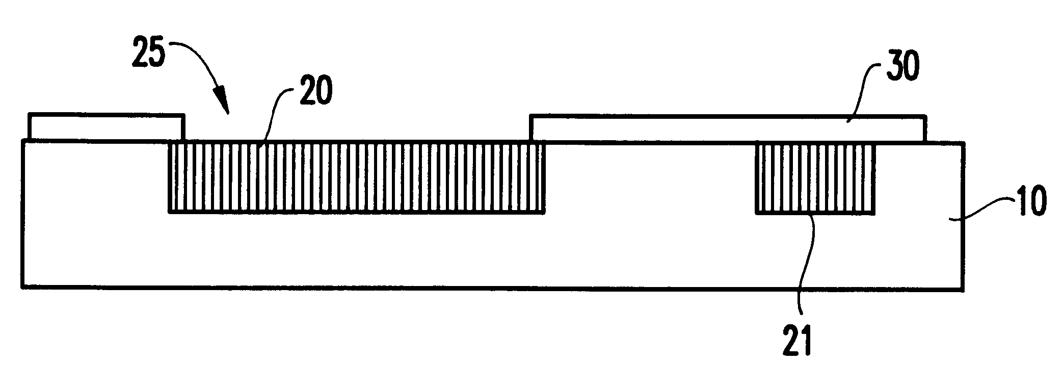
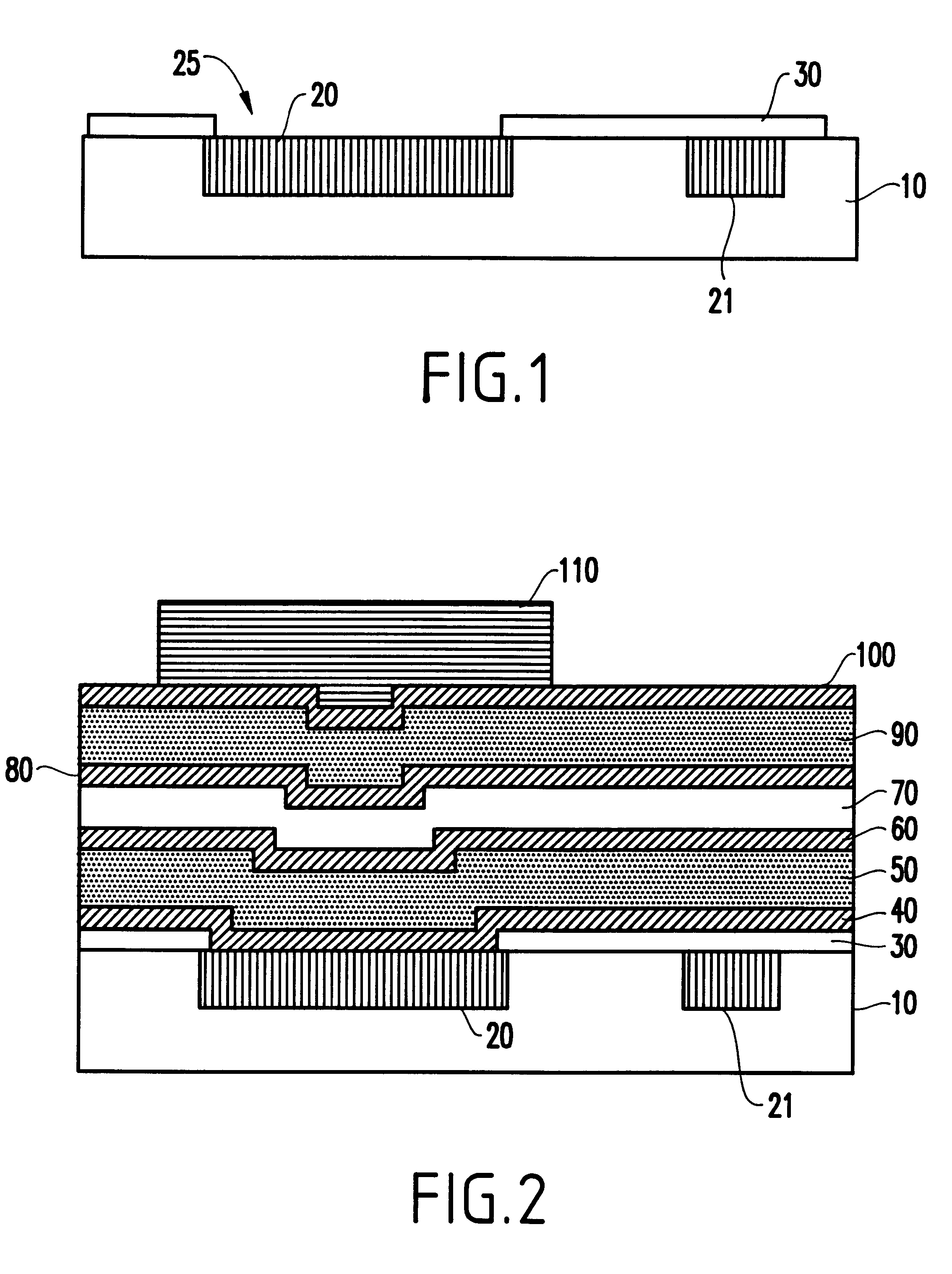
FIG. 1 shows a semiconductor substrate 10 such as a tantalum nitride substrate in which openings are formed using conventional masking and etching processes. A metal damascene layer 20 is then deposited in the openings and the structure is planarized using, for example, chemical mechanical polishing (CMP). In the preferred embodiment, the metal damascene layer 20, 21 is copper although other metals (such as gold) are also within the scope of this invention. Subsequently, a silicon nitride (Si.sub.3 N.sub.4) layer 30 is provided over the copper damascene layer 20, 21 and the semiconductor substrate 10. The silicon nitride layer 30 is subsequently masked and etched in the areas where the metal-insulator-metal capacitor will be provided and where the via will be formed. FIG. 1 shows a gap area 25 in the silicon nitride layer 30 where the metal-insulator-metal capacitor will be formed.

FIG. 2 shows the metal-insulator-metal capacitor formed over the copper damascene layer 20. As shown in...


PUM


Abstract

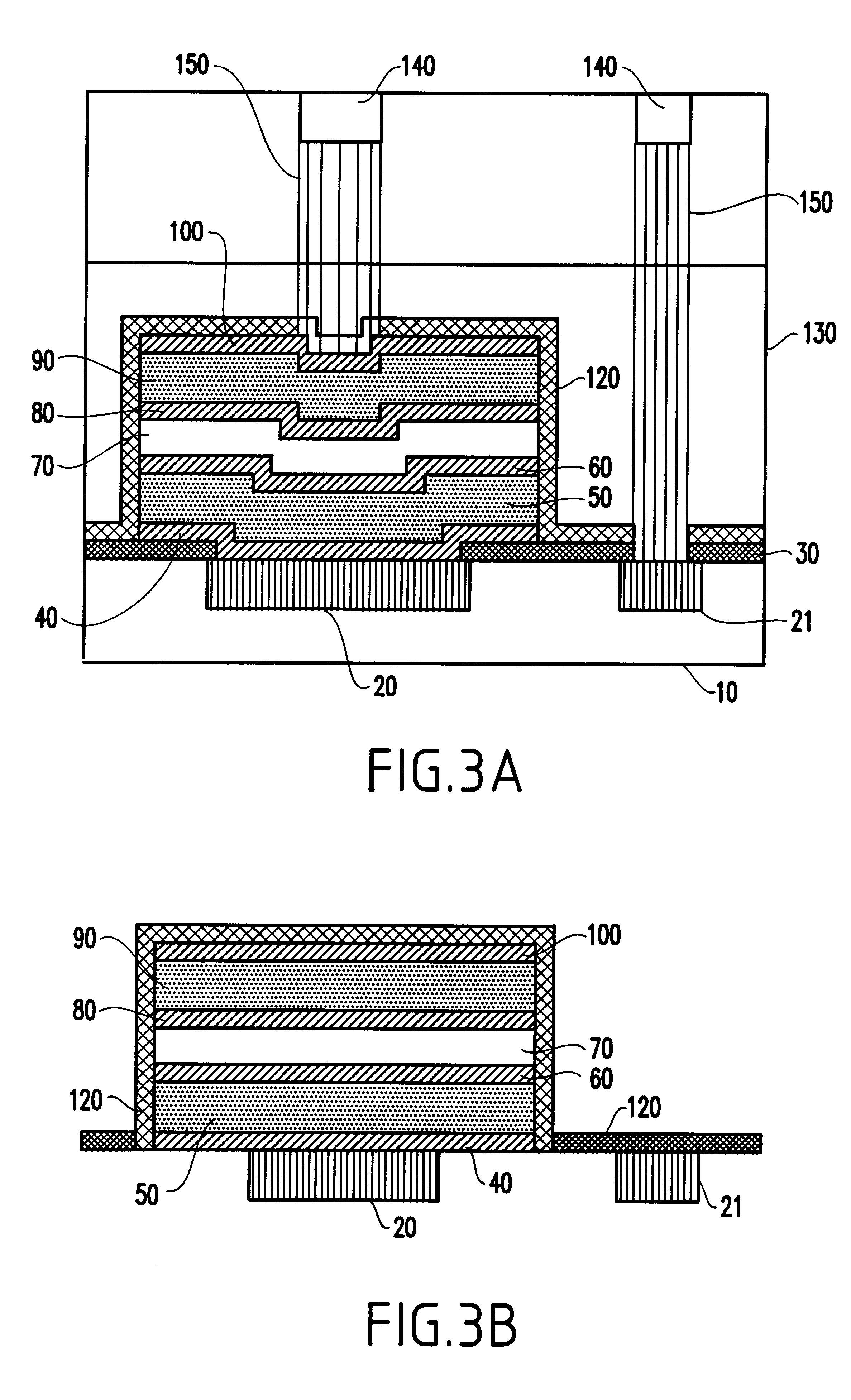
A capacitor structure formed on a semiconductor substrate may include a first interconnect wiring (such as copper damascene) and a first conductive barrier layer in contact with the first interconnect wiring. A first capacitor plate, a capacitor dielectric structure and a second capacitor plate may also be included over the first conductive barrier layer. A second conductive barrier layer may be formed on the second capacitor plate and a second planar insulating structure may be formed over the second capacitor plate. Finally, a second interconnect wiring may be embedded within a second planar insulator structure.

Description

1. Field of the InventionThe present invention generally relates to a metal-insulator-metal capacitor for a metal damascene process and a method of manufacturing the same.2. Description of the Related ArtPrecision capacitors for complementary metal oxide semiconductor (CMOS) analog applications are generally metal-insulator-metal (MIM) capacitors or polysilicon-insulator-polysilicon (P-P) capacitors.However, P-P capacitors are becoming less popular because they present a number of problems when used with complementary metal oxide semiconductor (CMOS) technologies. More specifically, P-P capacitors are generally performed before the CMOS structures and the heat and oxidation cycles which occur during the CMOS production process degrade the P-P capacitors. Further, the sophistication of analog circuits is improving which requires that the variation in the capacitance be decreased and preferably maintained at a voltage of approximately 25 ppM. However, P-P capacitors suffer from carrie...

Claims


Application Information

Patent Timeline
IPC IPC(8): H01L21/02H01L21/768H01L21/70
CPCH01L28/60
Inventor ADLER, ERICTROMBLEY, HENRY W.
Owner IBM CORP
Learn More