Method and apparatus for controlling photolithography parameters based on photoresist images

a technology of photoresist and parameters, applied in the field of photolithography techniques, can solve the problems of affecting the quality of photoresist materials,

Inactive Publication Date: 2001-07-10
GLOBALFOUNDRIES INC
View PDF2 Cites 112 Cited by
  • Summary
  • Abstract
  • Description
  • Claims
  • Application Information

AI Technical Summary

Problems solved by technology

Certain photoresist materials do not complete the transition from being soluble to being insoluble in the developer based solely on the exposure to light.
A limitation of a post develop measurement technique is that significant time elapses between the measurement and the corrective action, potentially resulting in numerous unusable wafers.

Method used


Image

  • Method and apparatus for controlling photolithography parameters based on photoresist images
  • Method and apparatus for controlling photolithography parameters based on photoresist images
  • Method and apparatus for controlling photolithography parameters based on photoresist images

Examples


Embodiment Construction

Illustrative embodiments of the invention are described below. In the interest of clarity, not all features of an actual implementation are described in this specification. It will of course be appreciated that in the development of any such actual embodiment, numerous implementation-specific decisions must be made to achieve the developers' specific goals, such as compliance with system-related and business-related constraints, which will vary from one implementation to another. Moreover, it will be appreciated that such a development effort might be complex and time-consuming, but would nevertheless be a routine undertaking for those of ordinary skill in the art having the benefit of this disclosure.

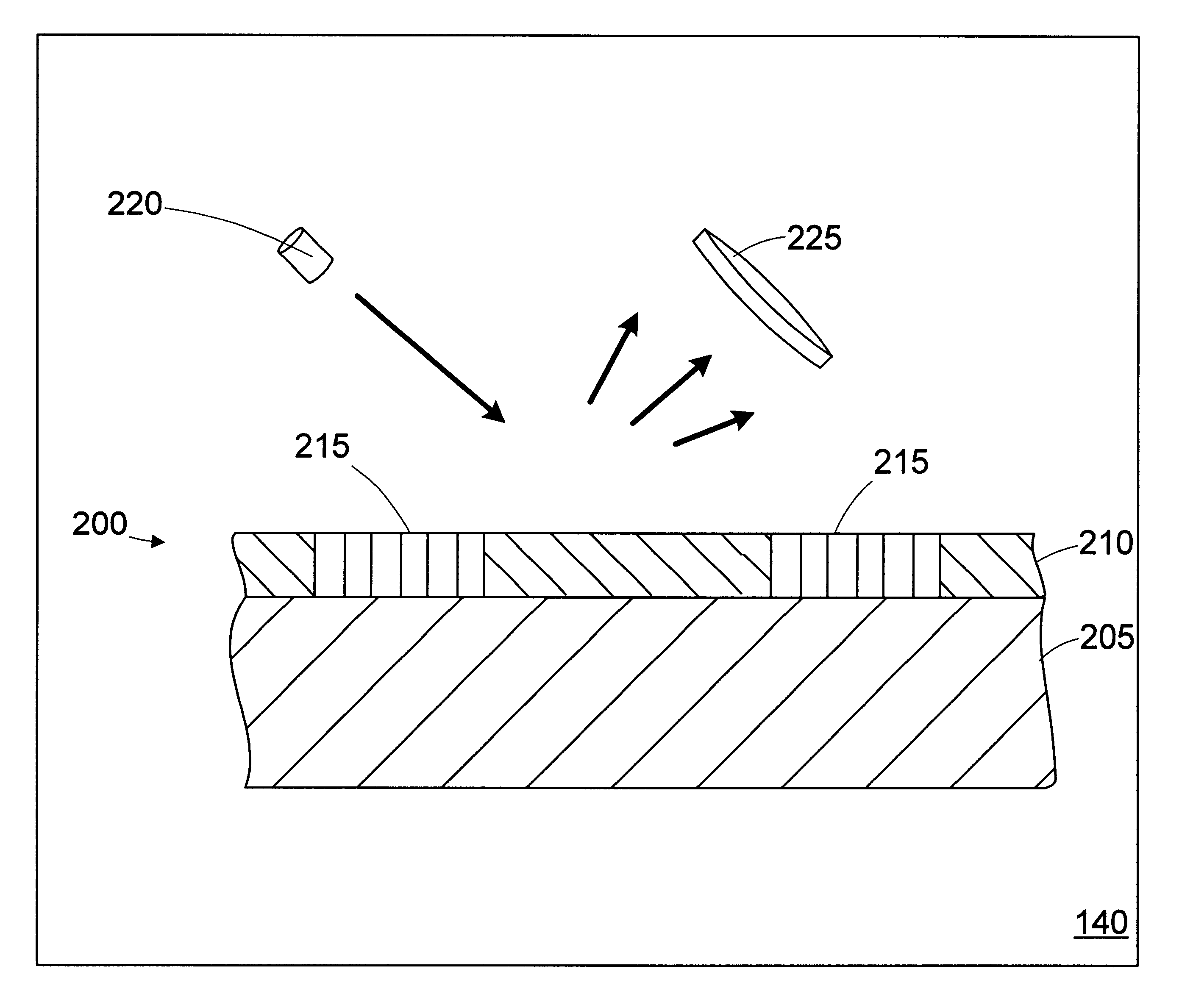
Referring now to the figures, and in particular, to FIG. 2, a simplified diagram of an illustrative processing line 100 for performing photolithography patterning is provided. The processing line 100 includes a stepper 110, an oven 120, a cool down station 130, a scatterometer 140, and...


PUM

PropertyMeasurementUnit
timeaaaaaaaaaa
light intensityaaaaaaaaaa
period of timeaaaaaaaaaa

Abstract

A method for controlling uniformity in a wafer is provided. A wafer is provided. A layer of photoresist is formed on the wafer, and the photoresist layer is patterned. A portion of the patterned photoresist layer is illuminated in at least first and second positions. Light reflected at the two positions is measured to generate first and second measurements. A recipe of a stepper is adjusted in response to the first measurement differing from the second measurement. A wafer processing system includes a stepper, a scatterometer, and a process controller. The stepper is adapted to expose a layer of photoresist in accordance with a recipe to generate an exposed layer of photoresist. The scatterometer is adapted to take first and second measurements in at least first and second positions on the exposed layer of photoresist. The process controller is adapted to compare the first and second measurements and adjust the recipe based on the first and second measurements.

Description

1. Field of the InventionThis invention relates generally to photolithography techniques for patterning semiconductor devices, and, more particularly, to a method and apparatus for controlling photolithography parameters based on photoresist images.2. Description of the Related ArtConventionally, semiconductor devices are patterned using photolithographic processes. A base material, such as a substrate material, a metal, an insulator, etc., is coated with a light sensitive material, referred to as a photoresist material. The photoresist is generally a composition that is sensitive to active rays of light, such as ultraviolet rays, X-rays or electron rays. The photoresist is deposited on the base material to selectively protect non-process portions of the substrate. Light is then selectively directed onto the photoresist film through a photomask, or reticle, to form photoresist patterns on the base material. The photoresist is then developed to remove either the exposed photoresist o...

Claims


Application Information

Patent Timeline
Patent Type & Authority Patents(United States)
IPC IPC(8): G03F7/20
CPCG03F7/70616G03F7/70558
Inventor MILLER, MICHAELGOODWIN, GREG
Owner GLOBALFOUNDRIES INC
Why Eureka
Try Eureka