Z-axis compressible polymer with fine metal matrix suspension

a metal matrix and compressible polymer technology, applied in the direction of dielectric characteristics, connection contact material, coupling device connection, etc., can solve the problems of time-consuming and therefore costly prior art techniques of providing conductive particles in an array that will insure particles at every contact pad of the device, and achieve the effect of reducing the number of openings

Inactive Publication Date: 2001-08-07
IBM CORP
View PDF13 Cites 105 Cited by
  • Summary
  • Abstract
  • Description
  • Claims
  • Application Information

AI Technical Summary

Benefits of technology

is to provide an electronic module which has a substantial reduction in opens between interconnections caused by camber.

Problems solved by technology

In the manufacture and assembly of electronic modules, deformities on the substrate surface make interconnection difficult.
Too many particles may lead to shorts while too few particles may not provide an adequate conductive pathway.
Prior art techniques of providing conductive particles in an array that will insure particles at every contact pad of the devices is time consuming and therefore costly.

Method used


Image

  • Z-axis compressible polymer with fine metal matrix suspension
  • Z-axis compressible polymer with fine metal matrix suspension
  • Z-axis compressible polymer with fine metal matrix suspension

Examples


Embodiment Construction

)

In describing the preferred embodiment of the present invention, reference will be made herein to FIGS. 1-2B of the drawings in which like numerals refer to like features of the invention. Features of the invention are not necessarily shown to scale in the drawings.

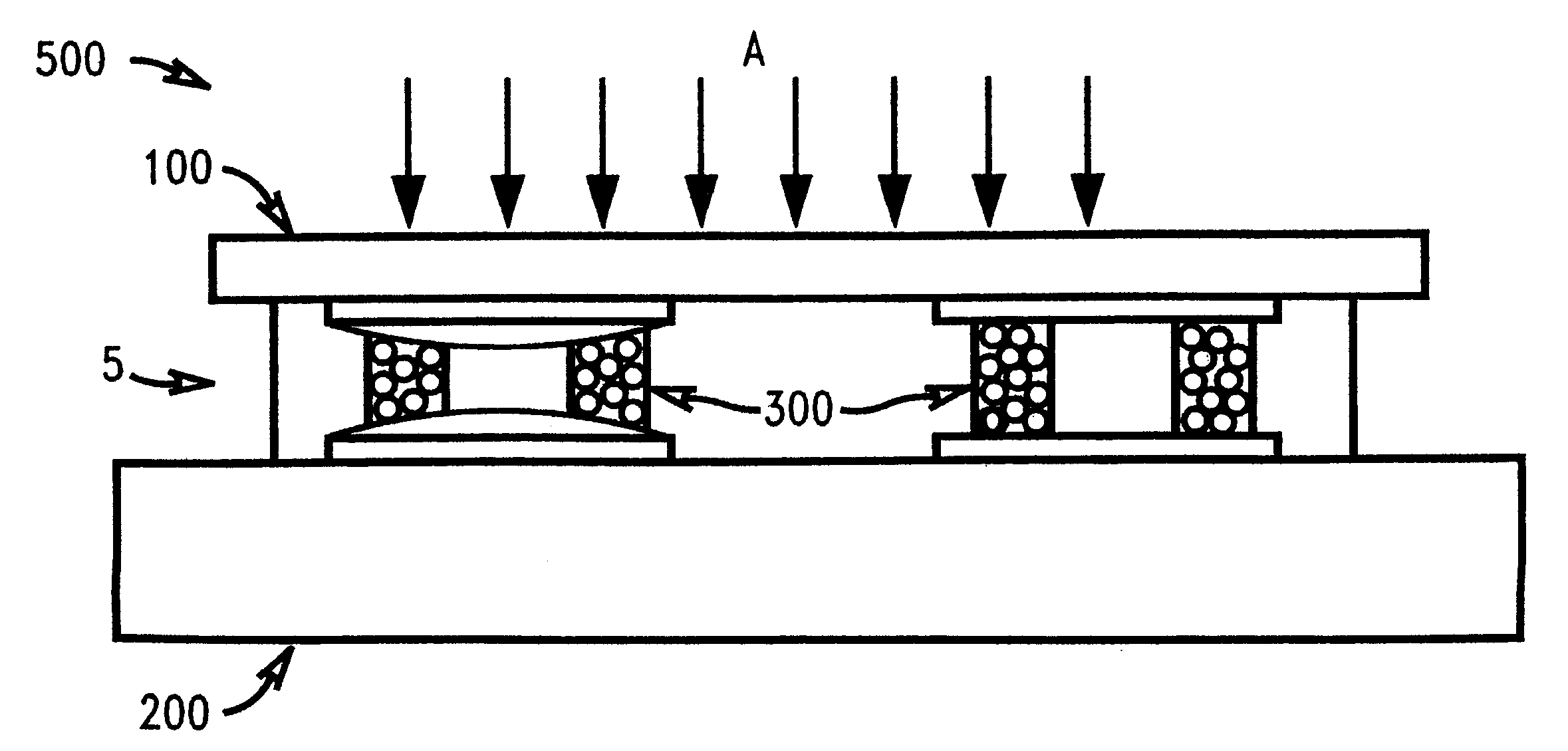
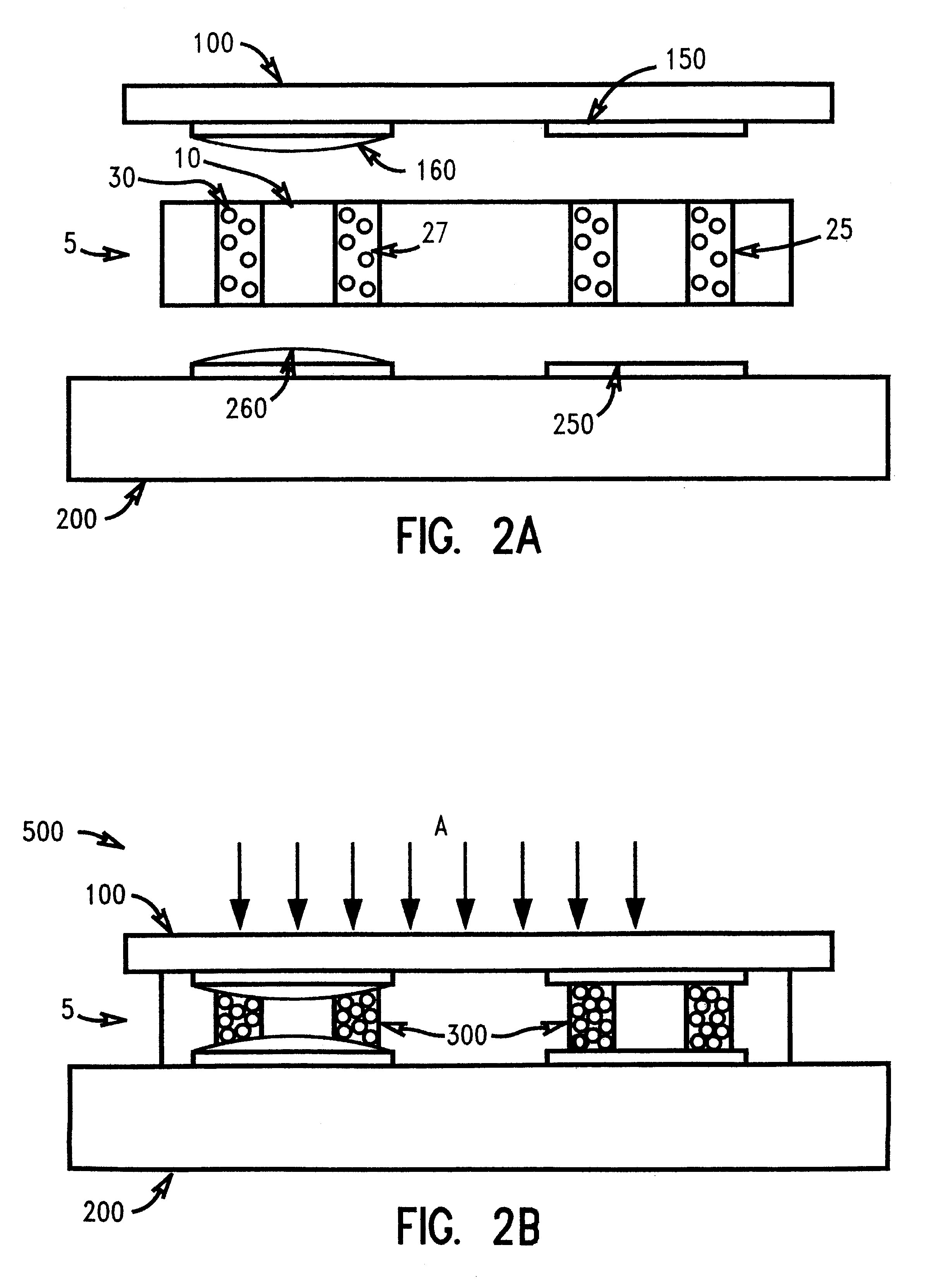
The present invention compensates for the camber found on electronic components by using a compressible interposer for interconnecting electronic components when forming an electronic module. The interposer of the present invention has a plurality of apertures filled with a dielectric material having a substantially uniform suspension of conductive particles therein. Upon compression of the interposer, the conductive particles contact each other to provide electrical interconnection between contact pads on the electronic components in a substantially z-axis direction.

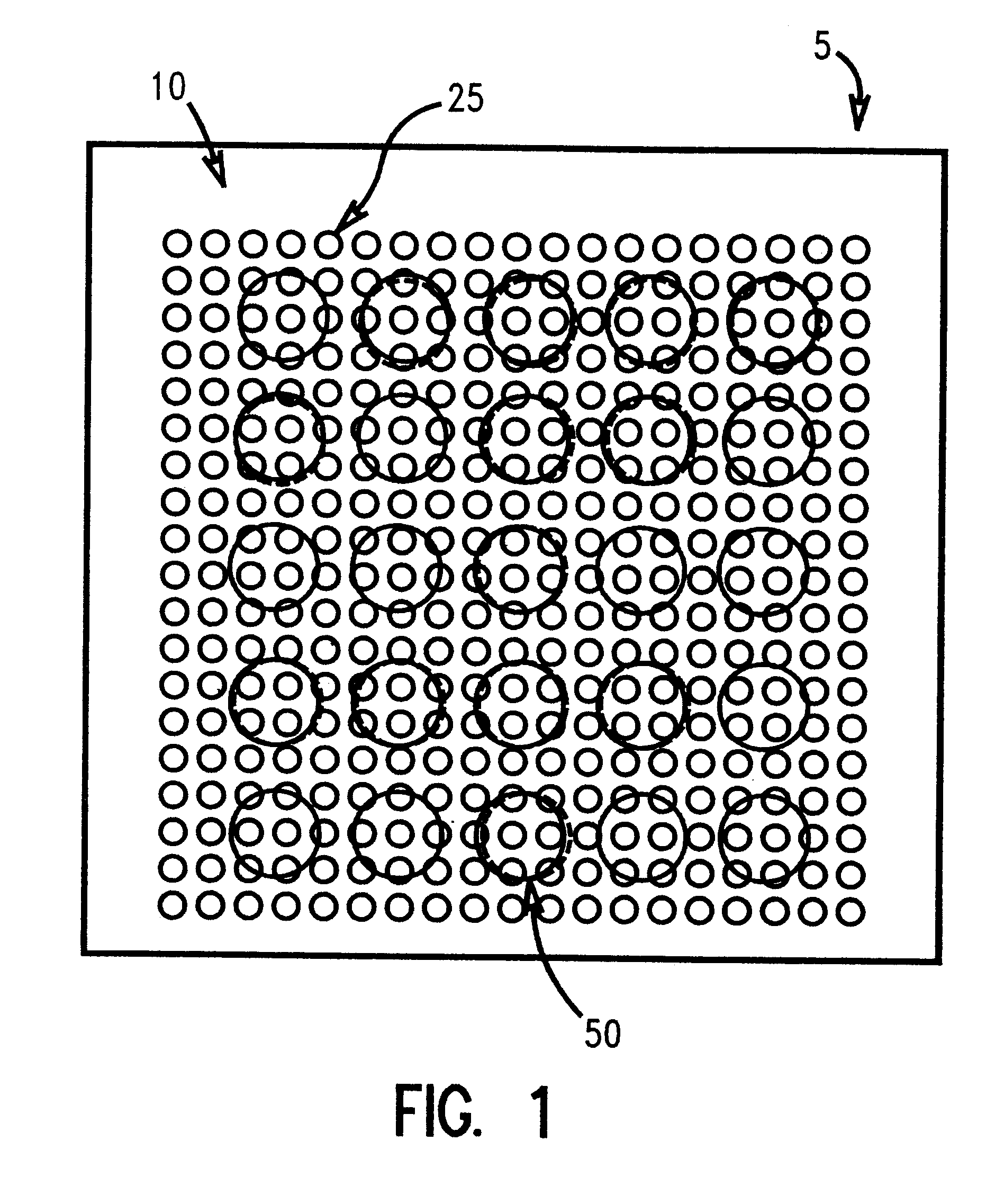
FIG. 1 is a top plan view of an interposer 5 of the present invention. Interposer 5 comprises an interposer sheet 10 having a plurality of apertures 25. Int...


PUM

PropertyMeasurementUnit
diameteraaaaaaaaaa
thicknessaaaaaaaaaa
temperatureaaaaaaaaaa

Abstract

A compressible interposer comprising an interposer sheet having a plurality of apertures filled with a dielectric material having a substantially uniform suspension of conductive particles therein forming a plurality of conductive sites. Preferably, the number of conductive sites on the interposer are greater in number than the number of contact pads on the electronic components such that precise alignment of the interposer between the electronic components is not required. The apertures of the interposer sheet confine the conductive particles within the dielectric material such that during compression of the interposer between the electronic components, z-axis conductive pathways are formed without shorting in the x and y directions. Preferably, the interposer sheet comprises polyimide. Preferably, the dielectric material comprises polyimide-siloxane. Preferably, the conductive particles have a diameter of about 2 to about 20 mum and comprise of a material selected from the group consisting of copper, gold, silver, nickel, palladium, platinum, and alloys thereof. The particles may also be coated with an additional conductive material such as solder having a lower melting temperature. Most preferably, the conductive particles comprise solder coated copper particles. The conductive particles are present in an amount of about 30 to about 90 wt. % of the total weight of the conductive particles and the dielectric material.

Description

Aspects of the present invention are related to subject matter disclosed in co-pending applications entitled "Copper Stud Process For C4 Pads," Ser. No. 09 / 315,374 filed on even date herewith and assigned to the assignee of the present invention, the subject matter of which is hereby incorporated by reference.1. Field of the InventionThe present invention relates to a novel interposer for use in the assembly of electronic modules which accommodates the camber on the electronic components while providing improved interconnection.2. Description of Related ArtIn the manufacture and assembly of electronic modules, deformities on the substrate surface make interconnection difficult. Typical ceramic substrates exhibit about 25 to about 50 .mu.m camber as measured from a flat surface of the substrate. When a device with conventional solder ball interconnections is joined to such a substrate, some of the solder balls will not contact the melting pads leading to opens in the circuitry of the...

Claims


Application Information

Patent Timeline
Patent Type & Authority Patents(United States)
IPC IPC(8): H01R13/24H01R13/22H05K3/32H01R43/02H01R4/58
CPCH01L24/29H01L24/83H01R12/52H01R13/2414H05K3/321H01L2224/29101H01L2924/0665H01L2924/014H01L2924/01033H01L2924/01006H01L2224/2919H01L2224/16H01L2224/293H01L2224/83101H01L2224/8319H01L2224/838H01L2924/01005H01L2924/01027H01L2924/01029H01L2924/0103H01L2924/01039H01L2924/01046H01L2924/01047H01L2924/01049H01L2924/0105H01L2924/01051H01L2924/01075H01L2924/01078H01L2924/01079H01L2924/01082H01L2924/0781H01R43/0256H05K2201/0129H05K2201/0154H05K2201/0162H05K2201/0272H05K2201/0284H05K2201/09945H05K2201/10378H05K2203/0425H01L2924/00H01L2224/81101H01L2224/05573H01L2224/05568H01L2924/00014H01L2224/05599
Inventor BROFMAN, PETER J.KNICKERBOCKER, JOHN U.RAY, SUDIPTA K.STALTER, KATHLEEN A.
Owner IBM CORP
Why Eureka
Try Eureka