Multi-level DRAM trench store utilizing two capacitors and two plates

a trench store and capacitor technology, applied in the field of dynamic random access memory, can solve the problems of requiring an unacceptable chip size and economic cost, little design development available at the cell level, and a loss in manufacturing economy

Inactive Publication Date: 2001-08-28
IBM CORP
View PDF9 Cites 45 Cited by
  • Summary
  • Abstract
  • Description
  • Claims
  • Application Information

AI Technical Summary

Benefits of technology

It is a another object of the invention to provide a multilevel memory cell which can represent two bits in four quantized voltages using only one voltage supply (providing two logic level voltages) for writing to the cell, thus achieving an effective storage density of two lithographic squares per bit without a requirement for additional voltage source space and with enhanced performance.
It is further object of the invention to provide a multilevel memory cell which can represent three bits in eight quantized voltages using only two voltage sources (providing three voltages) for writing to the cell, thus achieving an effective storage density of one and one-third lithographic squares per bit (exclusive of additional voltage source circuitry).

Problems solved by technology

However, to advance from sixteen Megabit memory chips to the currently available sixty-four Megabit memory chips, little design development was available at the cell level and the increase in capacity was principally developed through reduced feature size regimes and increased chip area.
Consequently, some loss in manufacturing economy was encountered in the sixty-four Megabit generation of memory chips due principally to increased overhead of exposure systems capable of higher resolution and reduced number of chips per wafer.
While minimum feature size regimes of 0.1 micron and smaller are technically feasible at the present time and foreseeable for commercial production, to develop a further generation of memory chips having a capacity of 256 Megabits per chip or greater without a major improvement in memory cell design would clearly require an unacceptable chip size and economic cost while not fully realizing potential or particularly significant performance improvement.
However, to date, no such designs have been developed.
However, known multi-level store designs have required all quantized voltages to be supplied to a cell through a corresponding bit line, resulting in substantial drive circuit complexity and requiring substantial chip space to accommodate it (which is thus not available for storage cells).
Some performance penalty is also incurred due to the necessary digital-to-analog conversion for writing and to the difficulty of level discrimination (and, possibly, error detection and recovery as the number of stored voltage levels increases).
No alternative has been proposed which would allow avoidance of this complexity and performance penalty that would not consume substantial chip space and thus would not permit adequate increase in memory cell numbers to be realized even with a reduction of effective cell footprint or chip area per bit.
In other words, no known or proposed cell designs have significantly relieved the tradeoff between storage density and power supply complexity and the chip space necessary to accommodate that complexity.

Method used


Image

  • Multi-level DRAM trench store utilizing two capacitors and two plates
  • Multi-level DRAM trench store utilizing two capacitors and two plates
  • Multi-level DRAM trench store utilizing two capacitors and two plates

Examples


Embodiment Construction

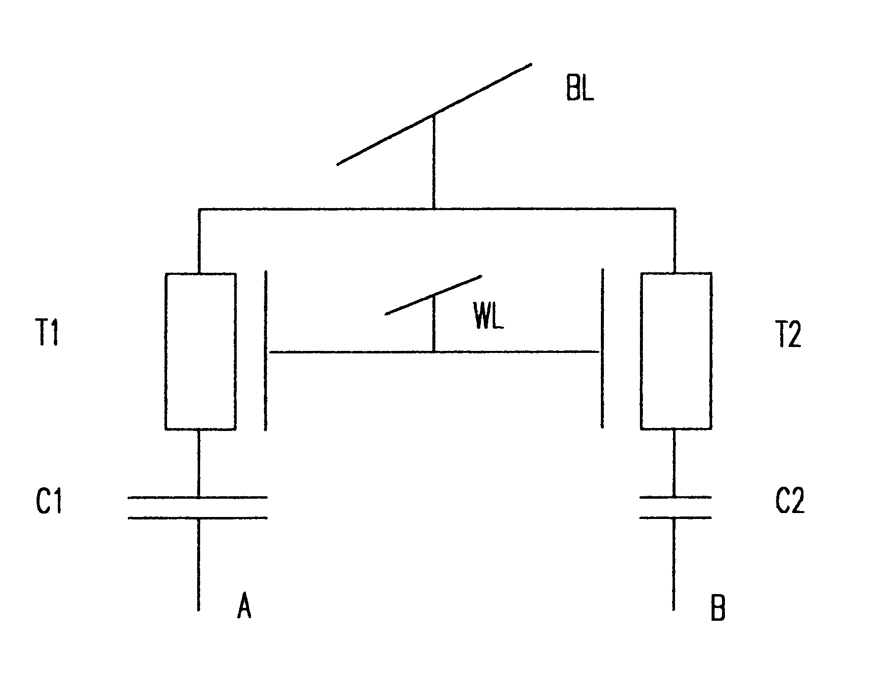
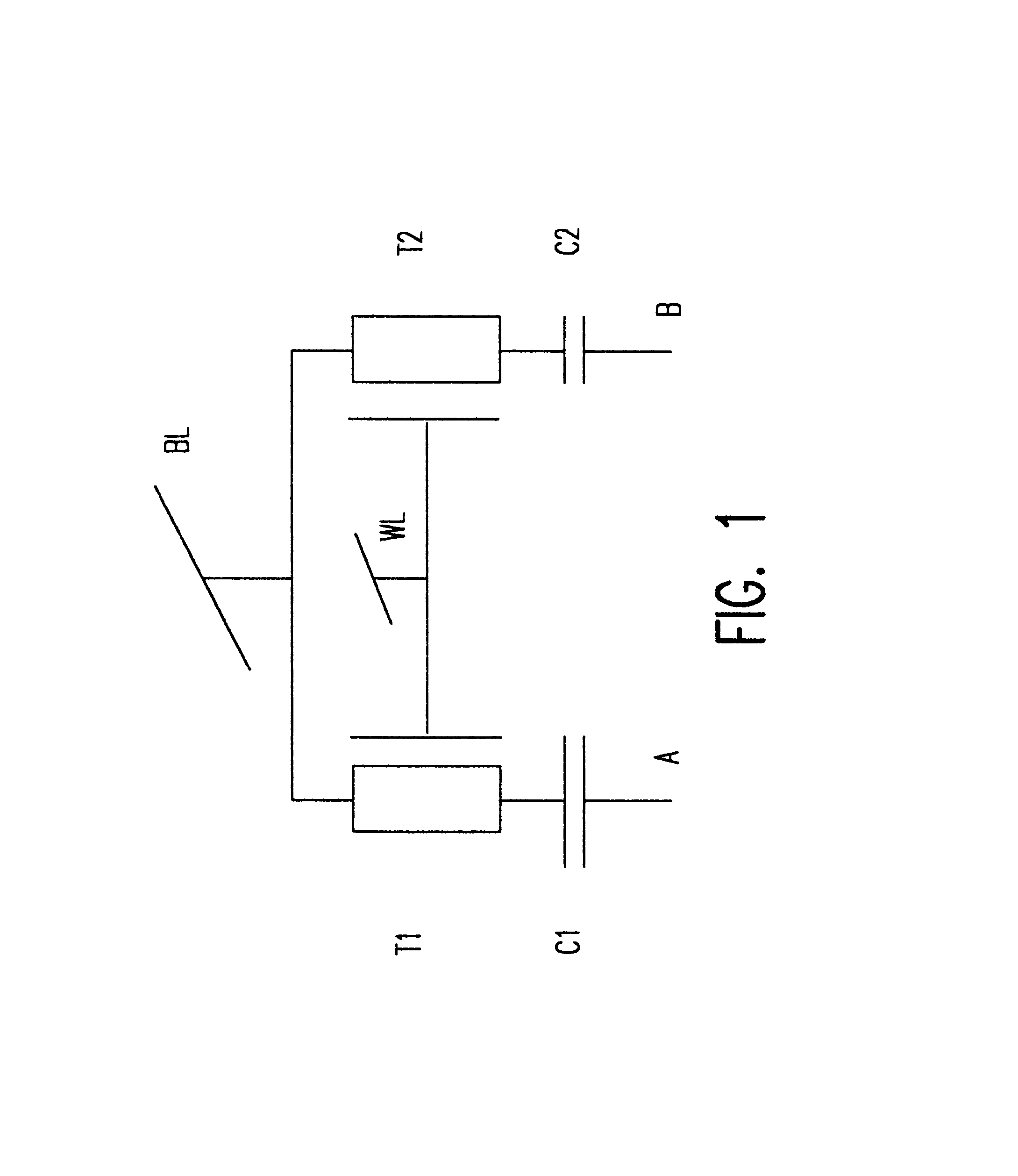
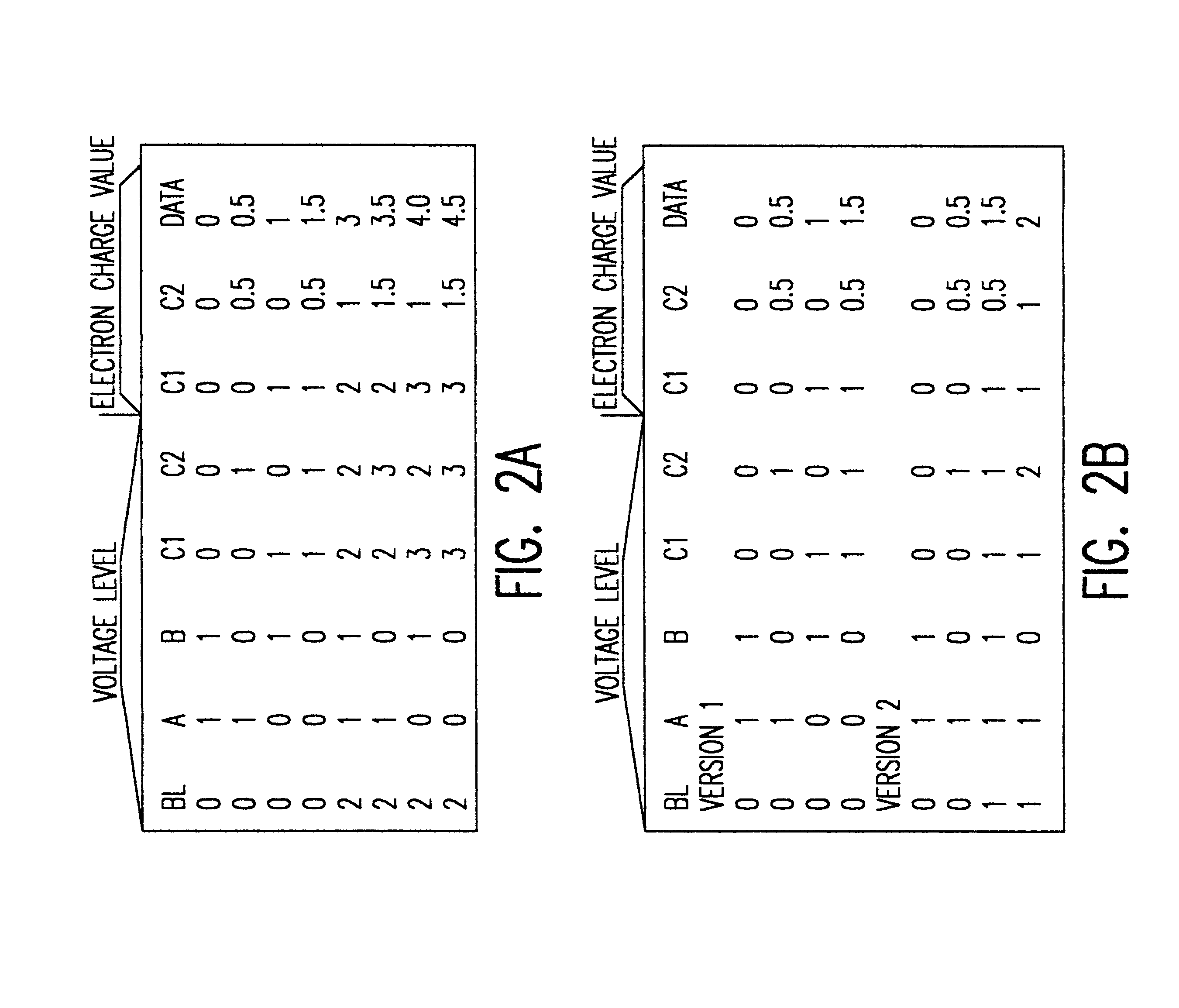
Referring now to the drawings, and more particularly to FIG. 1, there is shown a schematic diagram of a memory cell in accordance with the invention. The memory cell comprises two capacitors C1 and C2, each having a transistor, T1 and T2, respectively, connected in series therewith between a terminal of each capacitor and a bit line, BL. The transistors are controlled in common by having their gates commonly connected to a word line, WL. The other plate of the respective capacitors C1 and C2 is connected to a respective input A or B.

This latter feature of the invention is a departure from the design of known multi-level stores since known multi-level stores invariably rely on providing multiple voltage levels through the bit line; leading to substantial switching complexity as well as requiring multiple voltage level sources and possibly extended write, read, and cycle times if data is encoded as a combination of voltages on two or more capacitors (which must then be written sequent...


PUM


Abstract

A multi-level memory cell capable of storing two or three bits of digital data occupies only four lithographic squares and requires only one or two logic level voltage sources, respectively. High noise immunity derives from integration of the multi-level signal in the memory cell directly from logic level digital signals applied to two capacitors (as well as the bit line for the eight level mode of operation) by using capacitors having different values in order to avoid digital-to-analog conversion during writing. The capacitors can be simultaneously written and read to reduce memory cycle time. Transistor channels and capacitor connections are formed on adjacent semiconductor pillars using plugs of semiconductor material between pillars as common gate structures and connections. Opposite surfaces of the pillars also serve as storage nodes with common capacitor plates formed by conformal deposition between rows of plugs and pillars.

Description

1. Field of the InventionThe present invention generally relates to semiconductor storage structures and, more particularly, to dynamic random access memories of extremely high storage capacity fabricated on chips of limited size.2. Description of the Prior ArtIt is generally recognized that increased integration density in integrated circuits (ICs) provides benefits in both improved performance and manufacturing economy. Increased proximity of devices formed on a chip reduces connection length and capacitance; reducing signal propagation time and increasing noise immunity. Increased noise immunity may, in turn, allow reduction in operating voltages which allows further scaling of devices to smaller sizes on the chip. Increased integration density also allows more devices to be formed on a chip of given size using common wafer processing steps, allowing more chips to be formed with improved uniformity without significant increase of cost. To obtain these benefits, technology has dev...

Claims


Application Information

Patent Timeline
Patent Type & Authority Patents(United States)
IPC IPC(8): G11C11/56G11C11/403G11C11/404H01L27/108H01L21/70H01L21/8242
CPCG11C11/404G11C11/565H01L27/108H01L27/10882H01L27/10864H01L27/1087H10B12/00H10B12/0383H10B12/0387H10B12/48
Inventor FURUKAWA, TOSHIHARUHORAK, DAVID V.KALTER, HOWARD L.
Owner IBM CORP
Why Eureka
Try Eureka