Method for improving CMP processing

a technology of cmp and processing method, applied in the direction of basic electric elements, semiconductor/solid-state device manufacturing, electric apparatus, etc., can solve the problems of limited focus depth by the photolithographic system, metal residues during reactive ion etching, and patterning of subsequent layers

Inactive Publication Date: 2001-09-04
MICRON TECH INC
View PDF15 Cites 93 Cited by
  • Summary
  • Abstract
  • Description
  • Claims
  • Application Information

AI Technical Summary

Problems solved by technology

A nonplanar topography creates problems in the patterning of subsequent layers.
Such problems include, for example, limited depth of focus by the photolithographic system, metal residues during reactive ion etching, and poor metal step coverage.
However, conventional CMP creates micro scratches on the surface of the layer being polished.
These micro scratches are particularly problematic in interconnection schemes.
As dimensions of feature size becomes increasingly smaller, there is a greater probability that a scratch contacting adjacent metal lines may exist.
The metal trapped in such a scratch creates a short between the adjacent metal lines with which it is in contact, thus rendering the device defective.
While improving the conductivity of the material, doping also damages the surface of the substrate.

Method used


Image

  • Method for improving CMP processing
  • Method for improving CMP processing
  • Method for improving CMP processing

Examples


Embodiment Construction

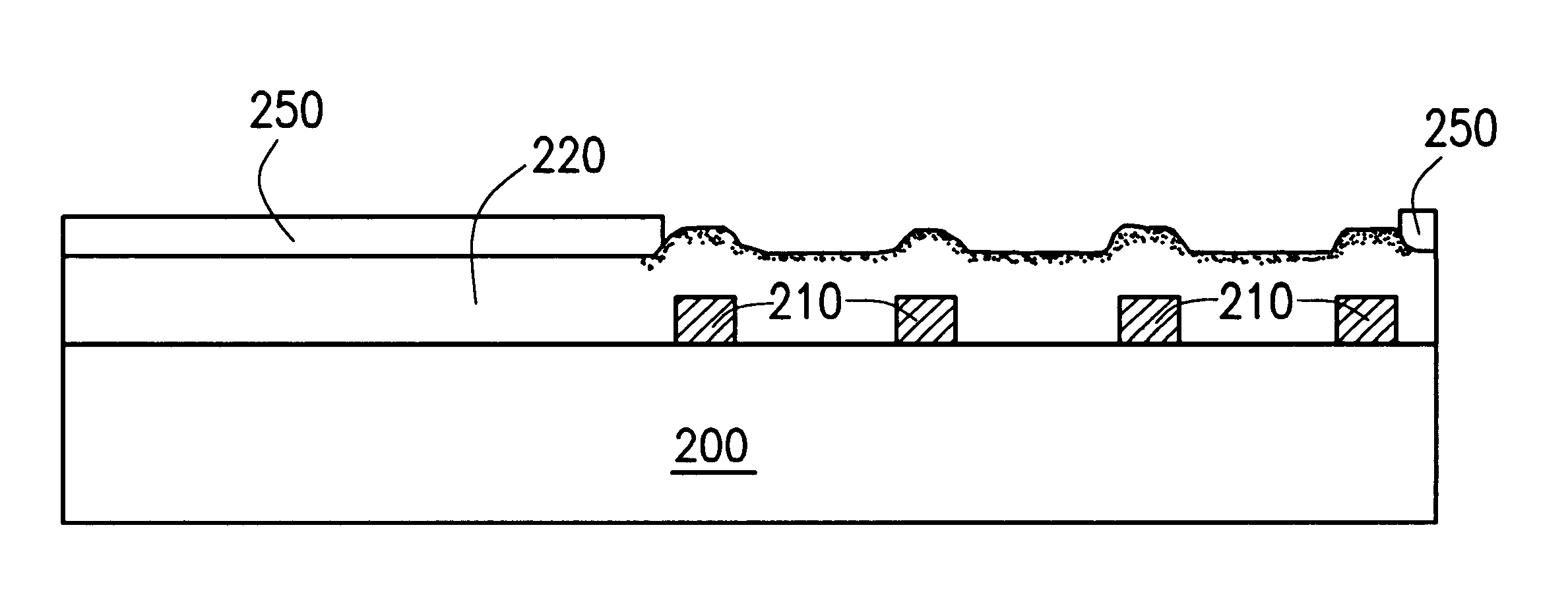
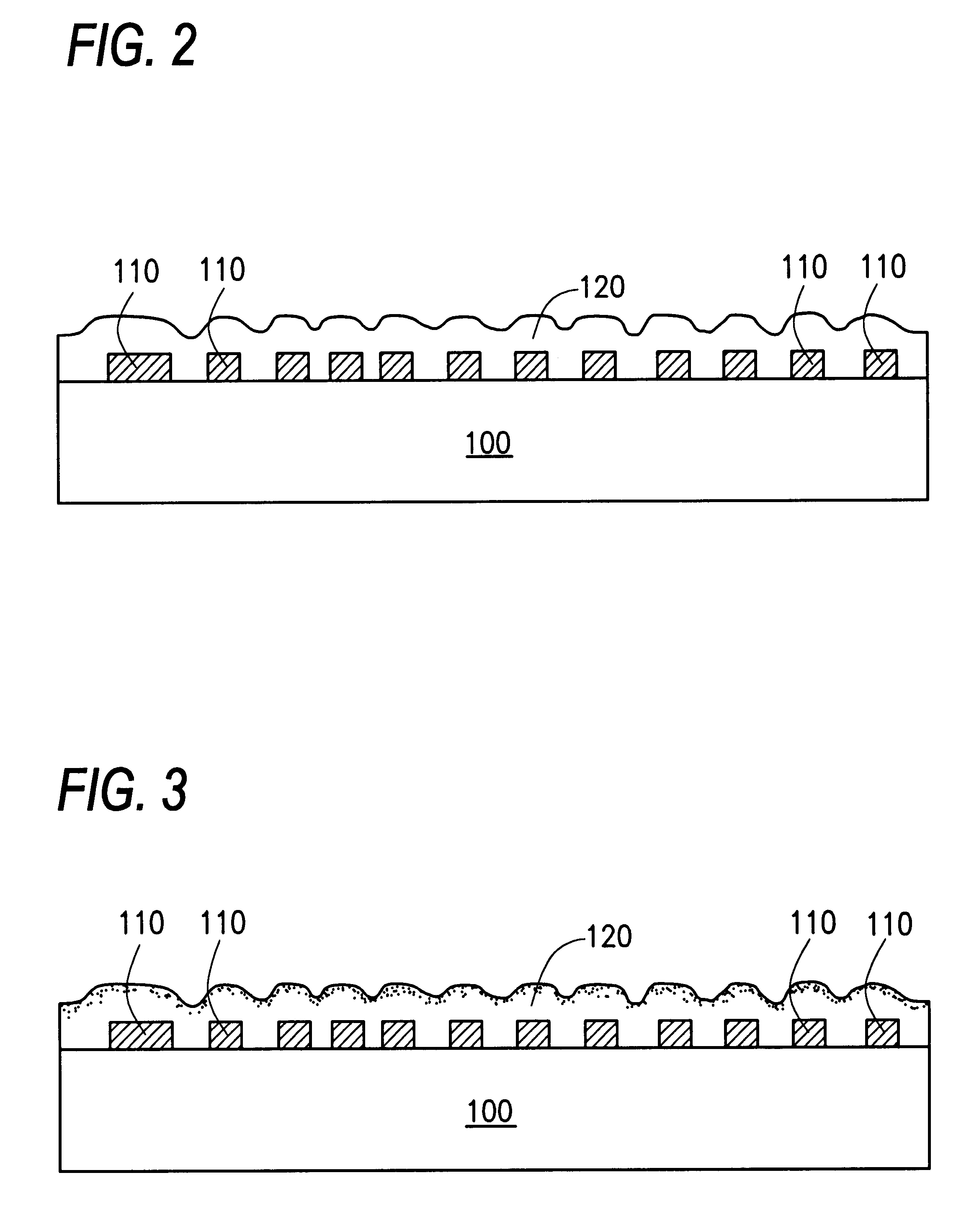
specific exemplary use of the invention is in the formation of shallow trench isolations regions is shown in FIGS. 10A through 10D. A wafer has deposited thereon a layer of oxide, e.g. silicon dioxide, and a layer of nitride. After a trench is defined, as shown in FIG. 10B, the wafer has a layer of silicon dioxide deposited thereon, as shown in FIG. 10B. The silicon dioxide layer is then implanted with phosphorus with a dopant concentration of from about 1.times.10.sup.15 ions / cm.sup.2 to about 1.times.10.sup.17 ions / cm.sup.2 by ion implantation at an energy of about 10 to 100 KeV, shown in FIG. 10c. The doped surface layer of the silicon dioxide layer is then CMP processed, as shown in FIG. 10d. The doped silicon dioxide layer can be removed faster and with less defects than comparable non-doped surfaces. The dosage and energy for the implant can be optimized to achieve the best process conditions. Other dopants as discussed above can also be used.

The above description and accompan...


PUM

PropertyMeasurementUnit
energyaaaaaaaaaa
concentrationaaaaaaaaaa
shallow trench isolation areaaaaaaaaaaa

Abstract

The invention also relates to an a method of fabrication of an integrated circuit, the method includes altering a portion of a surface layer of a material to be polished and polishing the surface layer in a chemical mechanical polishing process. Preferably, the step of altering of the present invention includes adding an impurity to the material such as a dopant by heavy ion implantation at a concentration level of about 1x10¹⁰ ions / cm2 to about 1x10¹⁸ ions / cm2.

Description

The invention relates generally to the fabrication of integrated circuits, and more particularly to structures and methods for improving the polishing steps in the fabrication of integrated circuits.DISCUSSION OF RELATED ARTIntegrated circuits are produced by fabricating hundreds of identical circuit patterns on a single semiconducting wafer which is subsequently divided into identical dies or chips. It is often desirable to provide a planar topography before a subsequent layer is formed. A nonplanar topography creates problems in the patterning of subsequent layers. Such problems include, for example, limited depth of focus by the photolithographic system, metal residues during reactive ion etching, and poor metal step coverage.A process commonly used in fabrication of integrated circuits to create a planar topography is chemical mechanical polishing (CMP). This process involves chemically etching of a surface while also mechanically grinding or polishing it. The combined action of...

Claims


Application Information

Patent Timeline
Patent Type & Authority Patents(United States)
IPC IPC(8): H01L21/02H01L21/321H01L21/3105
CPCH01L21/3212H01L21/31053
Inventor DOAN, TRUNG T.
Owner MICRON TECH INC
Why Eureka
Try Eureka