Lateral high-Q inductor for semiconductor devices

a semiconductor device and high-q technology, applied in the direction of transformers/inductance coils/windings/connections, basic electric elements, etc., can solve the problems of incompatible technology with the upper level copper metalization, inability to use the area subsequently for other circuitry, and inability to meet the requirements of semiconductor devices. achieve the effect of reducing the area requirements of the semiconductor devi

Inactive Publication Date: 2001-09-18
BELL SEMICON LLC +1
View PDF4 Cites 37 Cited by
  • Summary
  • Abstract
  • Description
  • Claims
  • Application Information

AI Technical Summary

Benefits of technology

It is therefore an object of the invention to provide a high-Q lateral inductor that provide reduced area requirements in a semiconductor device.

Problems solved by technology

This method has the disadvantage in that to create an inductor of 10, an area of typically more than 300 .mu.m.times.300 .mu.m is required.
This area subsequently cannot be used for other circuitry due to electromagnetic interference.
This processing results in inductors with air gaps that are not compatible with current processing technology.
Current versions of high-Q inductors on silicon substrates have been demonstrated with planar spiral inductors in AlCu, but this technology is not compatible with upper level copper metalization.

Method used


Image

  • Lateral high-Q inductor for semiconductor devices
  • Lateral high-Q inductor for semiconductor devices
  • Lateral high-Q inductor for semiconductor devices

Examples


Embodiment Construction

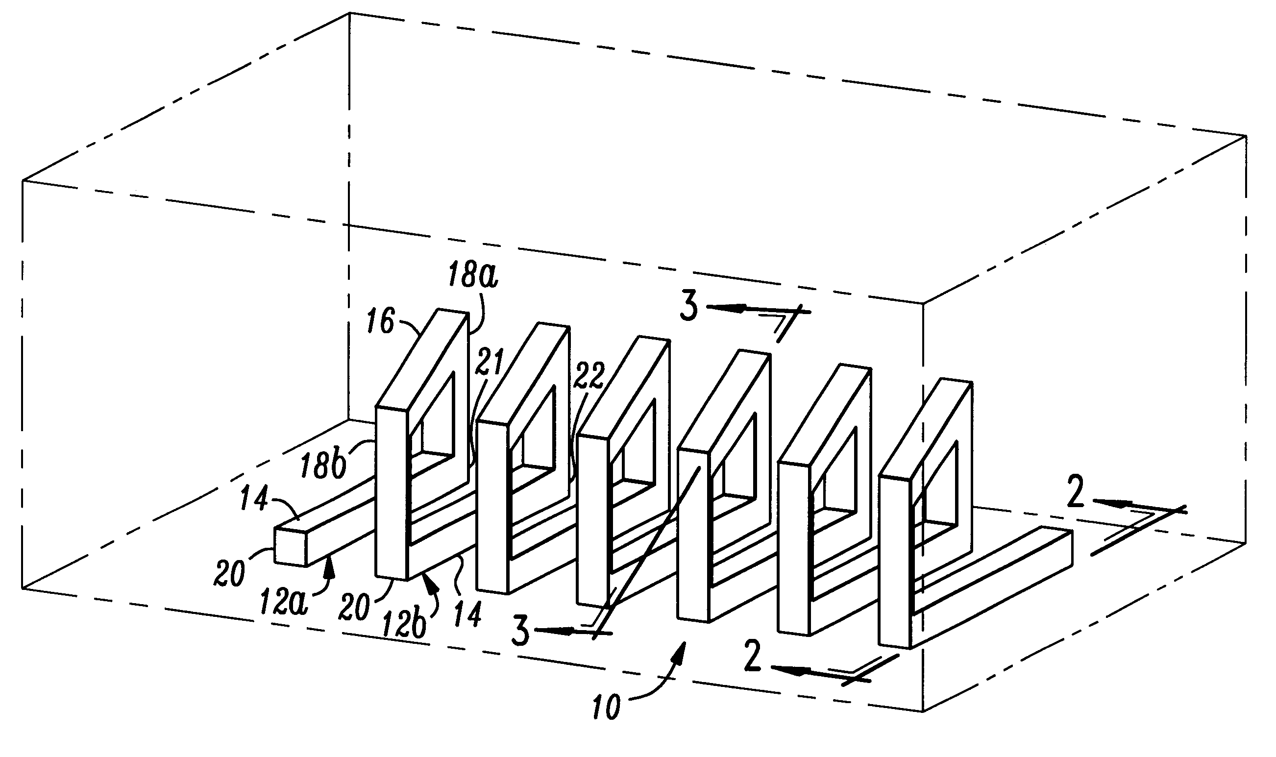
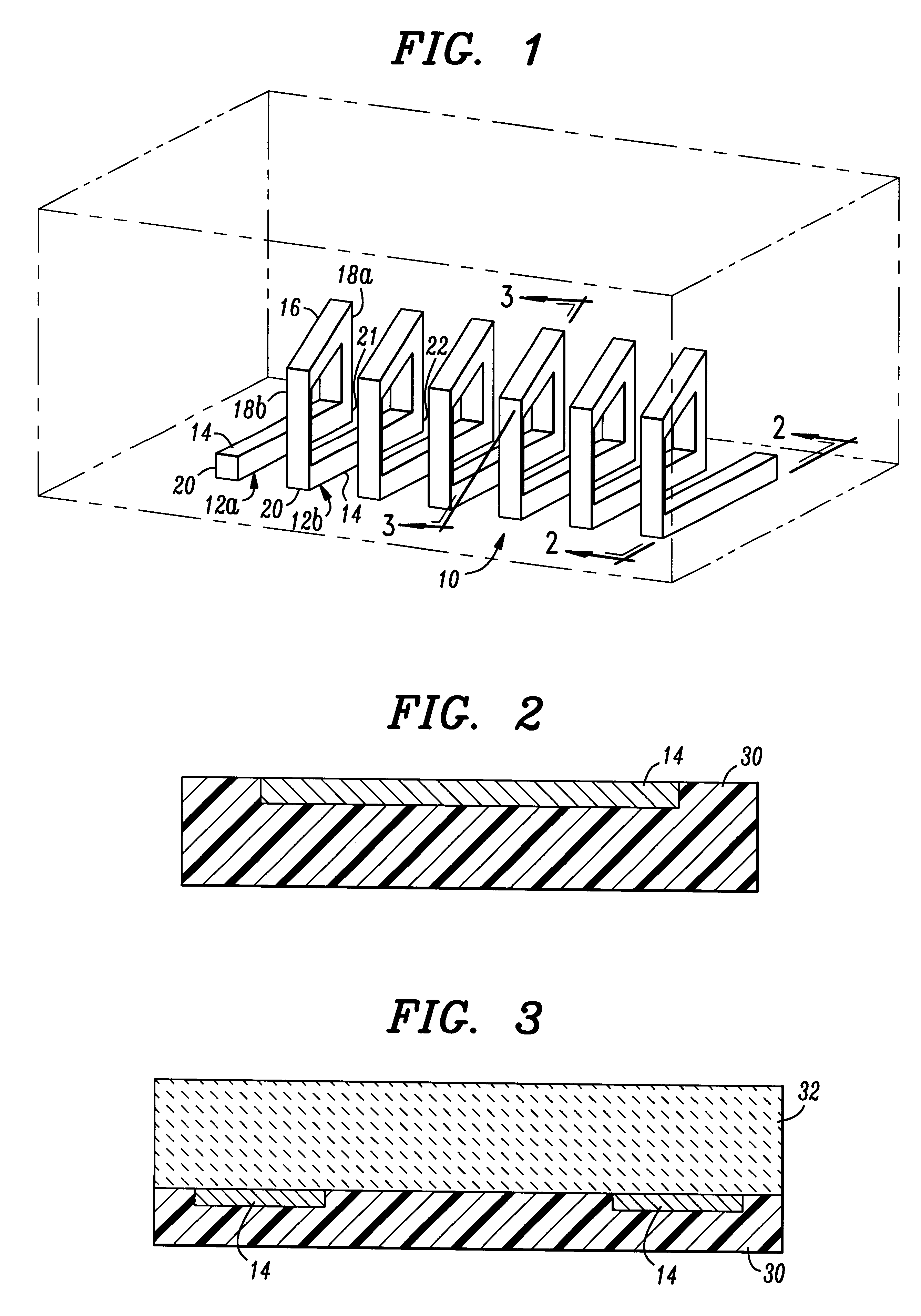
A lateral inductor for a semiconductor device according to the invention is illustrated in FIG. 1. The inductor 10 comprises a plurality of loops 12 connected in series along a lateral axis of the semiconductor device. The number of loops 12 for each inductor 10 is at least one and preferably two at a minimum and has no maximum number. Each loop 12 includes a bottom leg 14, a top leg 16, and a pair of side legs 18a, 18b. Between adjacent loops 12a, 12b, the second side leg 18b of the first loop 12a connects to the bottom leg 14 of the second loop. It being understood, however, the end point of one loop and the starting point of an adjacent loop need not occur between the second leg of the one loop and the bottom leg of the adjacent loop. Instead, the end point of one loop and the starting point of an adjacent loop can be at any point along the loop.

Although the bottom legs 14 of the inductor 10 can be oriented at any angle relative to one another, the bottom legs 14 of the inductor ...


PUM

PropertyMeasurementUnit
conductiveaaaaaaaaaa
areaaaaaaaaaaa
areasaaaaaaaaaa

Abstract

An inductor for a semiconductor device comprises a plurality of loops connected in series and formed along a lateral axis of the semiconductor device. Each loop comprises a bottom leg, a top leg, and a pair of side legs. The bottom legs are parallel and extend along a first plane. The top legs are also parallel and extend along a second plane. The second plane is parallel to and separate from the first plane. The first and second planes are parallel to said lateral axis, and the side legs are perpendicular to the first and second planes. The top and side legs can be formed from copper. A barrier layer between the top legs and a substrate layer adjacent the top legs and between the side legs and the bottom legs and the substrate layer can also be provided. The barrier can be formed from tantalum.

Description

CROSS-REFERENCE TO RELATED APPLICATIONNot ApplicableSTATEMENT REGARDING FEDERALLY SPONSORED RESEARCH AND DEVELOPMENTNot ApplicableFIELD OF THE INVENTIONThis invention relates to the manufacturing of semiconductor devices. More specifically, the invention relates to a lateral inductor on a semiconductor device.BACKGROUND OF THE INVENTIONHigh-Q inductors are a common feature found on most communications semiconductor devices. The most common method of forming an inductor in a semiconductor device involves depositing thick layers, 3 .mu.m or greater, of metal on the top layer of circuitry. This top layer is formed in a spiral pattern in conjunction with a special substrate to create a high-Q inductor. This method has the disadvantage in that to create an inductor of 10, an area of typically more than 300 .mu.m.times.300 .mu.m is required. This area subsequently cannot be used for other circuitry due to electromagnetic interference. Additionally, current processing techniques to form th...

Claims


Application Information

Patent Timeline
Patent Type & Authority Patents(United States)
IPC IPC(8): H01L23/52H01L23/64H01L23/522H01L23/58H01F41/04H01F17/00H01L21/822H01L27/02H01L27/04
CPCH01L23/5227H01L23/645H01L2924/0002H01L2924/00H01L27/02
Inventor CHU, JEROME TSU-RONG
Owner BELL SEMICON LLC
Why Eureka
Try Eureka