Semiconductor photonic element, method of fabricating the same, and semiconductor photonic device equipped therewith
- Summary
- Abstract
- Description
- Claims
- Application Information
AI Technical Summary
Problems solved by technology
Method used
Image

Examples
first embodiment
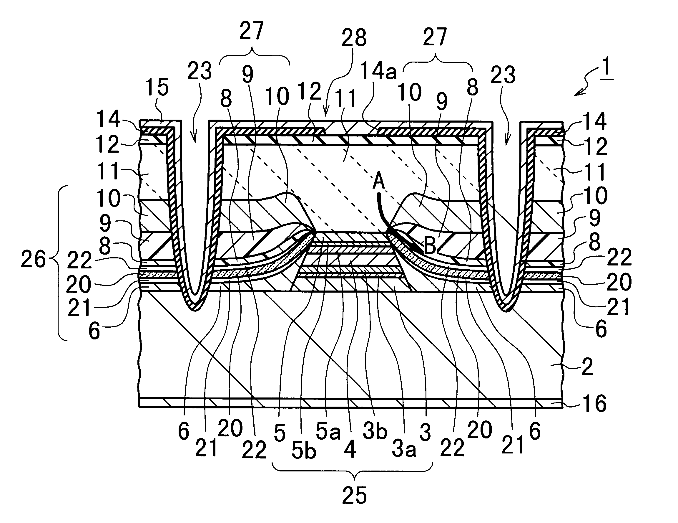
FIG. 5 shows the configuration of a semiconductor laser according to a
As shown in FIG. 5, the semiconductor laser 1 according to the first embodiment is comprised of an n-type InP substrate 2, a strip-shaped mesa structure 25 formed on an upper surface of the substrate 2, and a multilayer current-constricting structure 26 selectively formed on the surface of the substrate 2 at each side of the mesa structure 25. An optical waveguide forming the resonator of the laser is formed in the mesa structure 25 to extend along its axial direction.
The mesa structure 25 is formed by a p-type InP cladding layer 3 formed on the surface of the InP substrate 2, an n-type InGaAs guiding layer 3a formed on the layer 3, an n-type InGaAs guiding layer 3b formed on the layer 3a, an InGaAsP MQW active layer 4 formed on the layer 3b, a p-type InGaAs guiding layer 5a formed on the layer 4, a p-type InGaAs layer 5b formed on the layer 5a, and a p-type InP cladding layer 5 formed on the layer 5b. The active ...
second embodiment
FIG. 8B shows the configuration of a semiconductor laser 1A according to a second embodiment, which has the same configuration as that of the laser 1 according to the first embodiment of FIG. 5, except that a high-resistance semiconductor layer 31 is used instead of the p-type InP separation layer 6 and that another high-resistance semiconductor layer 32 is used instead of the combination of the three InP current-blocking layers 8, 9, and 10. Therefore, the explanation about the same configuration is omitted here for simplification of description by attaching the same reference symbols as those used in the first embodiment in FIG. 5.
Each of the high-resistance semiconductor layers 31 and 32 is an InP layer doped with Fe, where Fe is introduced into the layer 31 or 32 to increase the electric resistance. Thus, the layers 31 and 32 have a so-called semi-insulating property. Since the layers 31 and 32 have a level or levels for trapping electrons, they exhibit higher resistance than th...
third embodiment
FIG. 9 shows the configuration of a semiconductor photonic device 43, which is comprised of a Distributed-Feedback (DFB) laser 44a and an optical modulator 44b of the electric-field modulation type formed on the same n-type InP substrate 2. The DFB laser 44a has the same configuration as that of the semiconductor laser 1A according to the second embodiment of FIG. 8B and a diffraction grating 45 formed below the mesa structure 25. The mesa structure 25 including the active layer 4 is commonly used by the laser 44a and the modulator 44b, where the bandgap wavelength of the active layer 4 is changed in value between the laser 44a and the modulator 44b.
The reference numerals 15a and 15b denote the p-side electrodes of the DFB laser 44a and the optical modulator 44b, respectively. The n-side electrode 16 is commonly used by the laser 44a and the modulator 44b.
The semiconductor photonic device 43 having the above-described configuration according to the third embodiment is fabricated in ...
PUM
 Abstract
Description
Claims
Application Information
 - R&D Engineer
- R&D Manager
- IP Professional
- Industry Leading Data Capabilities
- Powerful AI technology
- Patent DNA Extraction
Browse by: Latest US Patents, China's latest patents, Technical Efficacy Thesaurus, Application Domain, Technology Topic.
© 2024 PatSnap. All rights reserved.Legal|Privacy policy|Modern Slavery Act Transparency Statement|Sitemap