Method of manufacturing a capacitor in a semiconductor device using a high dielectric tantalum oxide or barium strontium titanate material that is treated in an ozone plasma

Inactive Publication Date: 2001-12-11
HYUNDAI ELECTRONICS IND CO LTD
View PDF19 Cites 10 Cited by
  • Summary
  • Abstract
  • Description
  • Claims
  • Application Information

AI Technical Summary

Problems solved by technology

As the integration degree of a semiconductor device including DRAMs becomes higher, securing a sufficient static capacitance of a capacitor becomes problematic.
However, due to decrease of a process margin accompanied by the higher integration, there has been a limitation in increasing the surface area of the charge storage electrode.
Therefore, it may include large amount of carbon within the thin film and also may cause the defects of oxygen depletion upon deposition of the thin film.
Thus, it will increase a leak current to deteriorate the electric characteristic of the capacitor.
Even though, any post processing technology to overcome the

Method used


Image

  • Method of manufacturing a capacitor in a semiconductor device using a high dielectric tantalum oxide or barium strontium titanate material that is treated in an ozone plasma
  • Method of manufacturing a capacitor in a semiconductor device using a high dielectric tantalum oxide or barium strontium titanate material that is treated in an ozone plasma
  • Method of manufacturing a capacitor in a semiconductor device using a high dielectric tantalum oxide or barium strontium titanate material that is treated in an ozone plasma

Examples


Embodiment Construction

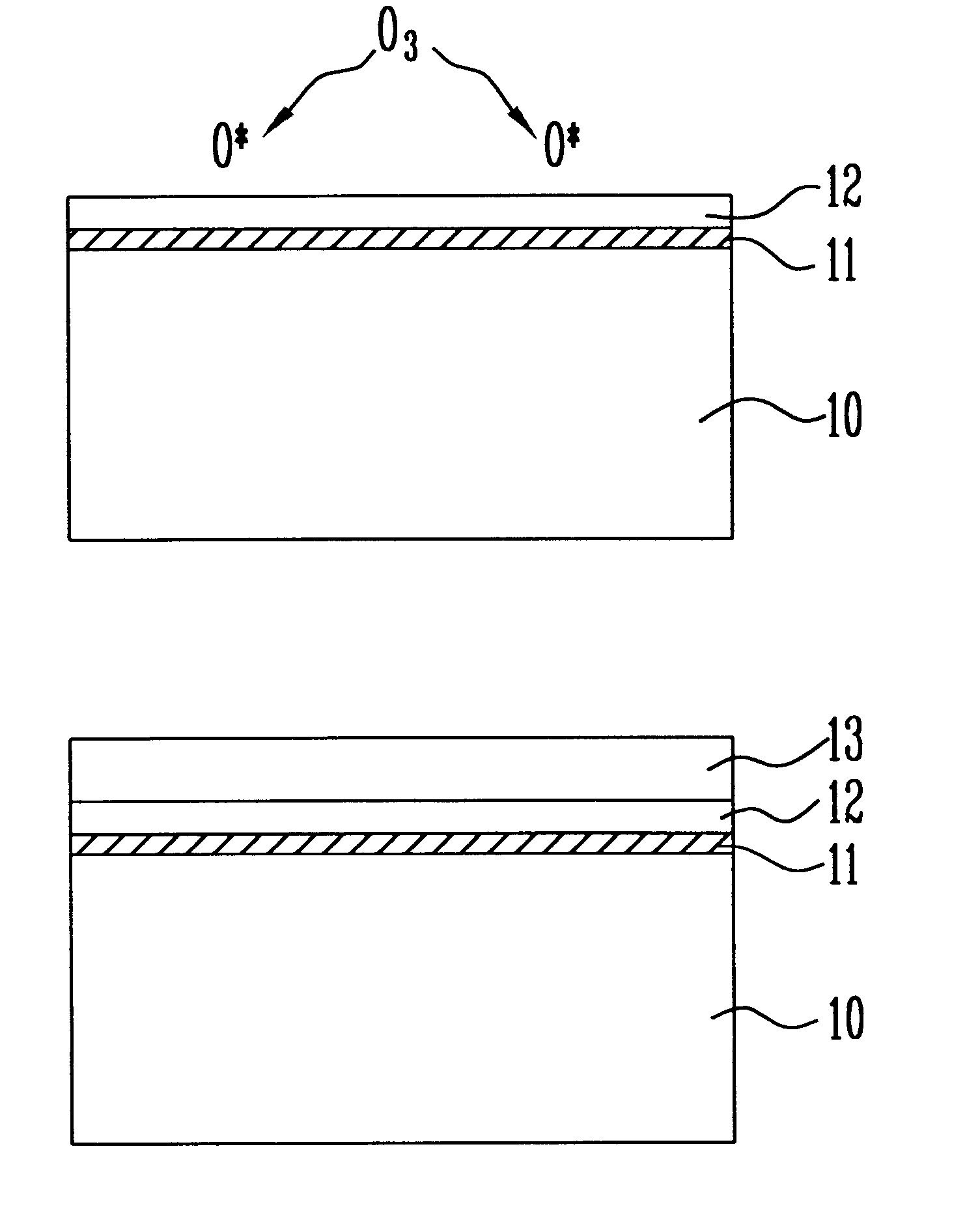
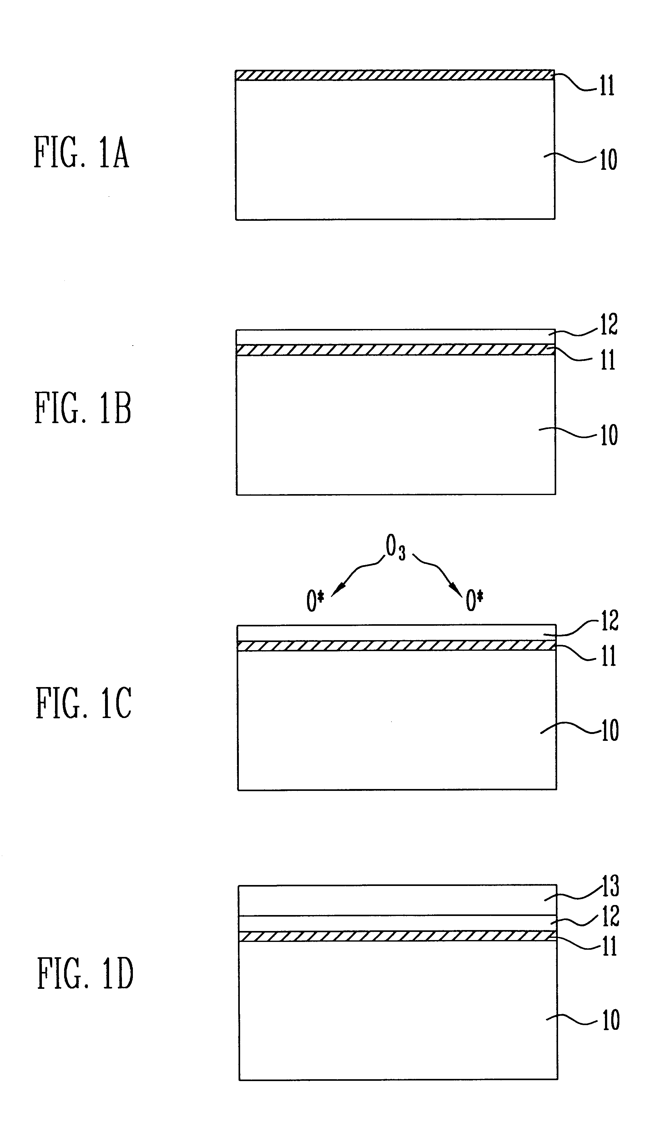
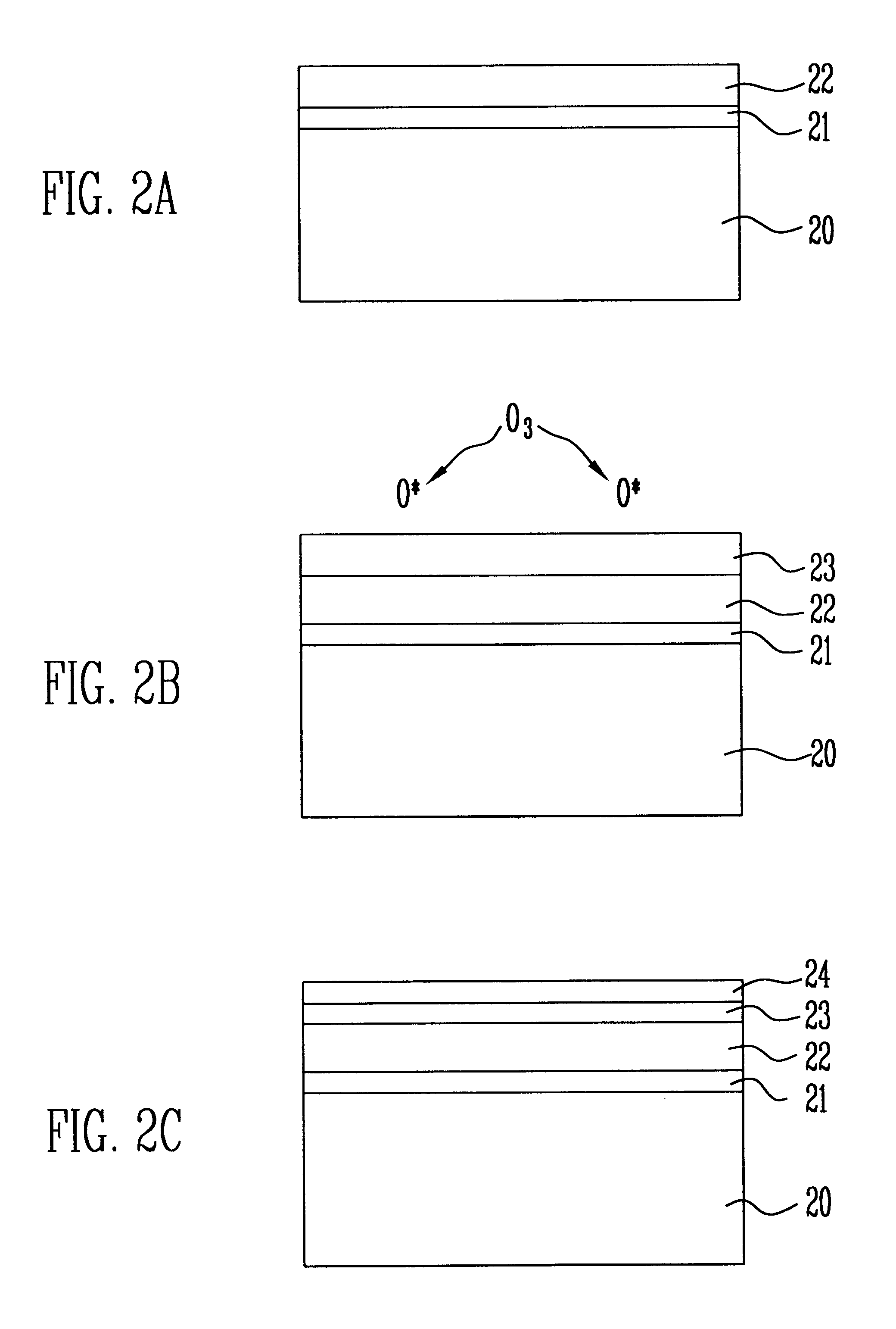
FIGS. 1a through 1d show the processes of manufacturing a tantalum oxide film capacitor according to one embodiment of the present invention.

First, as shown in FIG. 1a, an underlying polysilicon electrode 10 of a capacitor is formed on a substrate to which a given underlying process was finished. Then, a natural oxide film (not shown), which is formed on the surface of the underlying polysilicon electrode 10, is removed using HF or BOB (Buffered Oxide Etchant) solution. Next, the surface of the underlying polysilicon electrode 10 is nitrided by performing a rapid thermal nitridation (RTN) process at the temperature of 800 through 950.degree. C. At this time, the nitridation process for the underlying electrode 10 is to prevent the thickness of the effective oxide film of the capacitor from increasing since the surface of the underlying polysilicon electrode 10 is oxidized under a high temperature of oxygen atmosphere when and after Ta.sub.2 O.sub.3 is deposited. In the drawing, refe...


PUM

PropertyMeasurementUnit
Fractionaaaaaaaaaa
Fractionaaaaaaaaaa
Pressureaaaaaaaaaa

Abstract

There is disclosed a method of making a high dielectric capacitor of a semiconductor device using Ta2O5, BST((Ba1-xSrx)TiO3) etc. of a high dielectric characteristic as a capacitor dielectric film in a very high integrated memory device. The present invention has its object to provide a method of manufacturing a high dielectric capacitor of a semiconductor device, which can effectively remove carbon contained within the thin film after deposition of the BST film and defects of oxygen depletion caused upon deposition of the thin film and which can also remove carbon contained within the thin film after deposition of the tantalum oxide film and defects of oxygen depletion caused upon deposition of the thin film, without further difficult processes or without any deterioration of the electrical characteristic of the capacitor. It employs the technology which is able to effectively removing defects of carbon and oxygen depletion within the thin film, by forming a plasma O3 gas having a good reactivity and by processing the plasma for the BST thin film and tantalum oxide film. Thus, it can extend the lifetime of the activated oxygen of oxygen, which had been a problem in processing a conventional UV-O3, by means of plasma process using O3 gas. Therefore, it can effectively remove defects of carbon and oxygen within the BST thin film and tantalum oxide film without complicating the process or deteriorating the electrical characteristic of the capacitor. The present invention also proposes a detailed process condition, which can optimize the plasma process using O3 gas.

Description

1. Field of the InventionThe present invention relates to a semiconductor technology. In particular, the present invention relates to a method of making a high dielectric capacitor in a semiconductor device, in which Ta.sub.2 O.sub.5, BST((Ba.sub.1-x Sr.sub.x)TiO.sub.3) etc. having a high dielectric characteristic are used as capacitor dielectric films in a very high integrated memory device.2. Description of the Prior ArtAs the integration degree of a semiconductor device including DRAMs becomes higher, securing a sufficient static capacitance of a capacitor becomes problematic. As one of the solutions to solve this problem, a lot of efforts have been made to increase the surface area of the charge storage electrode, that is the underlying electrode of the capacitor. However, due to decrease of a process margin accompanied by the higher integration, there has been a limitation in increasing the surface area of the charge storage electrode.In order to overcome this limitation, inter...

Claims


Application Information

Patent Timeline
IPC IPC(8): C23C16/56C23C16/40H01L21/02H01L21/316H01L21/314H01L27/04H01L21/822H01L21/8242H01L27/108
CPCC23C16/405C23C16/409C23C16/56H01L21/31691H01L28/55H01L21/02205H01L21/02271H01L21/02183H01L21/02197H10B12/00H01L21/02356H01L21/0234
Inventor KIM, KYONG MINLIM, CHANLEE, KIL HOPARK, KI SEON
Owner HYUNDAI ELECTRONICS IND CO LTD
Why Eureka
Try Eureka