Apparatus and method for uniformly depositing thin films over substrates

Inactive Publication Date: 2002-01-15
ADVANCED ION BEAM TECHNOLOGY INC
View PDF6 Cites 31 Cited by
  • Summary
  • Abstract
  • Description
  • Claims
  • Application Information

AI Technical Summary

Benefits of technology

A thin film deposition apparatus and method are disclosed in this invention. The method includes a step of providing a vacuum chamber for containing a thin-film particle source for generating thin-film particles to deposit a thin-film on the substrates. The method further includes a step of containing a substrate holder in the vacuum chamber for holding a plurality of substrate having a thin-film deposition surface facing the thin-film particle source. The method further includes a step of providing a rotational means for rotating the substrate holder to rotate each of the substrates exposed to the thin-film particles for depositing a thin film thereon. And, the method further includes a step of providing a laterally moving means for laterally moving and controlling a duration of exposure time across a radial direction for each of the substrates for controlling a thickness uniformity of the thin-film deposited on each of the substrates.
A preferred embodiment of this in

Problems solved by technology

Several difficulties have been encountered by those of ordinary skill in the art for applying conventional apparatuses and methods for carrying out the task of thin film deposition on substrates, such as the optical thin film and the semiconductor wafers.
Specifically, even that the thin-film thickness may be critical for narrow band optical filters and integrated-circuit manufacture; a high degree of thin-film uniformity is not easily achievable.
Furthermore, the uniformity of thin-film thickness is generally not measured and also difficult to control.
However, as a more st

Method used


Image

  • Apparatus and method for uniformly depositing thin films over substrates
  • Apparatus and method for uniformly depositing thin films over substrates
  • Apparatus and method for uniformly depositing thin films over substrates

Examples


Example

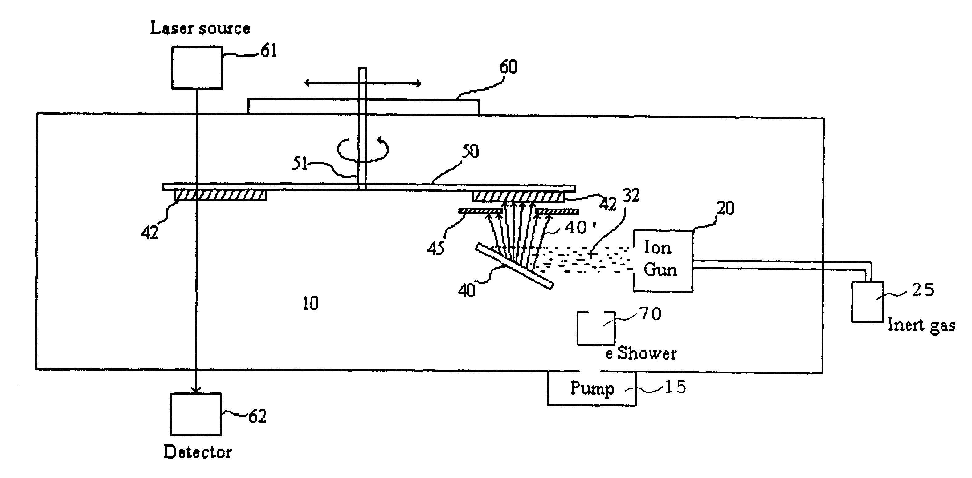
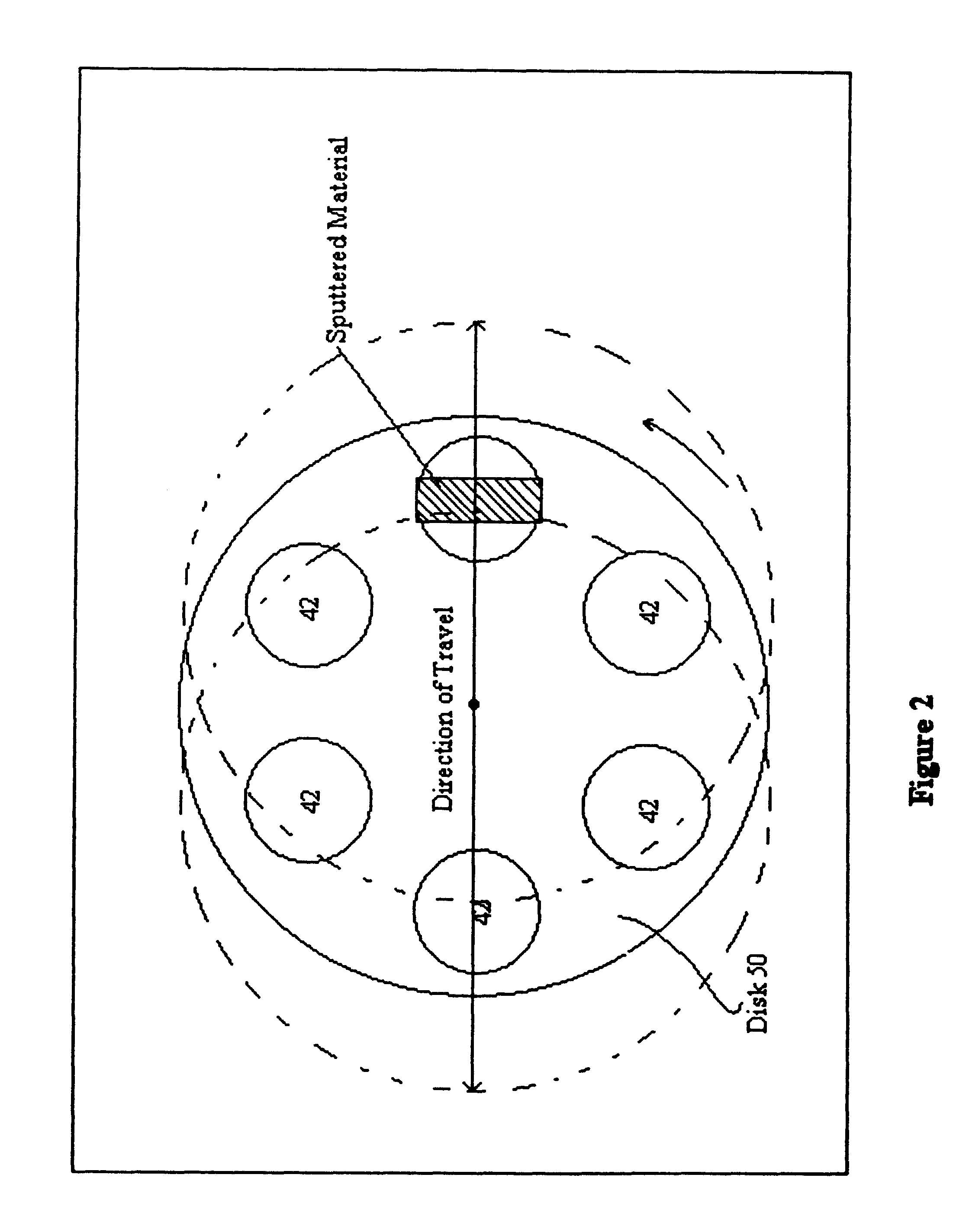
The present invention teaches a novel and improved thin-film deposition apparatus and method by employing a thickness detector to continuously monitor the thickness of the thin-film during a deposition process and applying combined rotational-and-lateral movements with controllable speed to control the uniformity of the thin-film thickness. FIG. 1 is a diagram for illustrating the system configuration for carrying out a thin-film deposition process provided with capabilities to control the uniformity of thin-film thickness. A vacuum chamber 10 for containing the thin-film deposition system is evacuated to a low air pressure by applying a vacuum pump 15. The ion guns 20 disposed inside the vacuum chamber 10 are supplied with inert gas from an inert gas source 25 to produce a positively charged ion beam 32. The targets 40 employed for thin film deposition are held at an acute angle to the ion beam 32 The ion beam impinges onto the targets 40 made of a thin-film deposition material for...


PUM

PropertyMeasurementUnit
Thicknessaaaaaaaaaa
Areaaaaaaaaaaa
Vacuumaaaaaaaaaa

Abstract

A thin film deposition apparatus and method are disclosed in this invention. The method includes a step of providing a vacuum chamber for containing a thin-film particle source for generating thin-film particles to deposit a thin-film on the substrates. The method further includes a step of containing a substrate holder in the vacuum chamber for holding a plurality of substrates having a thin-film deposition surface facing the thin-film particle source. The method further includes a step of providing a rotational means for rotating the substrate holder to rotate each of the substrates exposed to the thin-film particles for depositing a thin film thereon. And, the method further includes a step of providing a lateral moving means for laterally moving and controlling a duration of exposure time across a radial direction for each of the substrates for controlling thickness uniformity of the thin-film deposited on each of the substrates.

Description

1. Field of the InventionThe invention disclosed herein relates generally to method and apparatus for thin film deposition on optical thin film substrates, semiconductor wafers, and magnetic storage devices. More particularly, this invention relates to an improved apparatus and method for more uniformly depositing thin films on semiconductor wafers with materials sputtered from targets by collision of high-energy ion beams.2. Description of the Prior ArtSeveral difficulties have been encountered by those of ordinary skill in the art for applying conventional apparatuses and methods for carrying out the task of thin film deposition on substrates, such as the optical thin film and the semiconductor wafers. Specifically, even that the thin-film thickness may be critical for narrow band optical filters and integrated-circuit manufacture; a high degree of thin-film uniformity is not easily achievable. Furthermore, the uniformity of thin-film thickness is generally not measured and also d...

Claims


Application Information

Patent Timeline
IPC IPC(8): C23C14/54C23C14/46C23C14/50
CPCC23C14/46C23C14/547C23C14/505
Inventor CHEN, JIONG
Owner ADVANCED ION BEAM TECHNOLOGY INC
Why Eureka
Try Eureka