Photomask for near-field exposure having opening filled with transparent material
a near-field exposure and transparent material technology, applied in the field of photomasks, can solve the problems of high equipment cost and low throughput, low throughput, and high equipment cos
- Summary
- Abstract
- Description
- Claims
- Application Information
AI Technical Summary
Problems solved by technology
Method used
Image
Examples
first embodiment
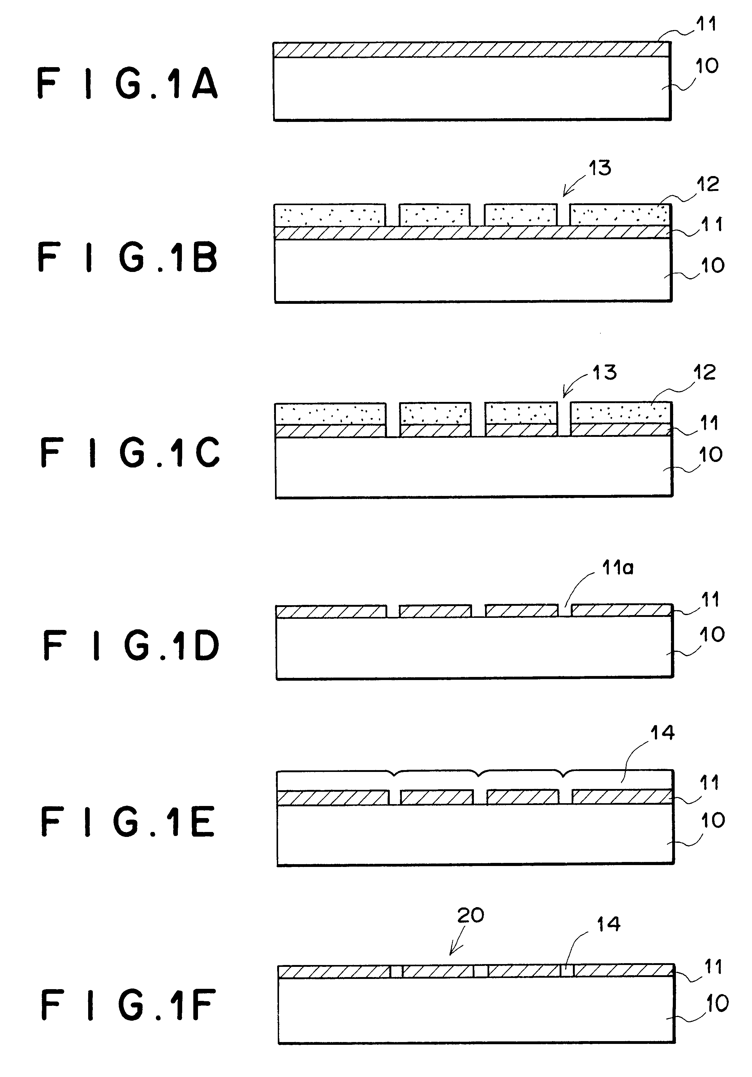
The process for producing a photomask for use in near-field exposure, as the first embodiment of the present invention, is explained below with reference to FIGS. 1A to 1F, which are cross-sectional views of the constructions in the initial, four intermediate, and final stages of the process.
In the first stage, a shading film 11 is formed on a surface of a mask support 10, as illustrated in FIG. 1A. The mask support 10 is made of a flat quartz glass plate. For example, the shading film 11 is made of a chromium film having a thickness of 50 nm and a chromium oxide film having a thickness of 50 nm.
In the second stage, first, the shading film 11 is coated with an electron beam resist, which is then baked. Next, portions of the electron beam resist, corresponding to a predetermined pattern, are exposed to an electron beam, and post exposure baking (PEB) is performed. Thereafter, a developing operation is performed on the electron beam resist by using a special developer, so that a resis...
second embodiment
The process for producing a photomask for use in near-field exposure, as the second embodiment of the present invention, is explained below with reference to FIGS. 3A to 3F, which are cross-sectional views of the constructions in the initial, four intermediate, and final stages of the process. The same reference numerals as in FIGS. 1A to 1F are assigned to the elements in FIGS. 3A to 3F which are substantially the same as the corresponding elements in FIGS. 1A to 1F.
In the first stage, a surface of a mask support 10 undergoes HMDS (hexamethyle disilazane) treatment for enhancing adhesiveness. Then, the surface of the mask support 10 is coated with an electron beam resist 30 as illustrated in FIG. 3A, and the electron beam resist 30 is baked. Next, for the purpose of charge-up elimination, gold is deposited to a thickness of about 10 nm by vacuum evaporation.
In the second stage, portions of the electron beam resist, corresponding to a predetermined pattern, are exposed to an electro...
third embodiment
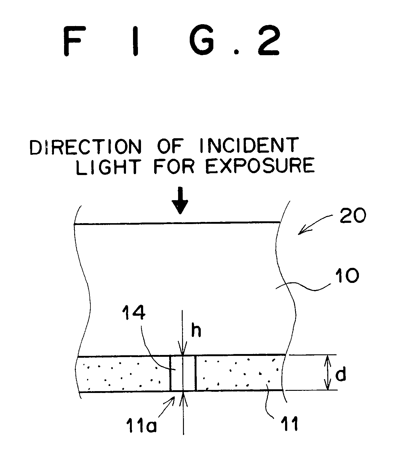
As explained above, in each of the first and second embodiments, the height of the filler or protruding portion above the level of the boundary between the mask support and the shading film is identical with the thickness of the shading film. However, in the third embodiment of the present invention, the height of the filler or protruding portion above the level of the covered portions of the mask support is different from the thickness of the shading film.
FIG. 5 is a magnified cross-sectional view of the photomask 50 as the third embodiment of the present invention. In the photomask 50 of FIG. 5, the height h" of the filler or protruding portion above the level of the covered portions of the mask support is smaller than the thickness d" of the shading film, i.e., h"
PUM
| Property | Measurement | Unit |
|---|---|---|
| height | aaaaa | aaaaa |
| thickness | aaaaa | aaaaa |
| heights | aaaaa | aaaaa |
Abstract
Description
Claims
Application Information


