Optical signal power monitor and regulator

a technology of optical signal and power monitor, which is applied in the direction of lasers, semiconductor amplifier structures, semiconductor lasers, etc., can solve the problems of attenuation of optical signals, and limited dynamic range of optical receivers

Inactive Publication Date: 2002-02-12
II VI DELAWARE INC
View PDF5 Cites 63 Cited by
  • Summary
  • Abstract
  • Description
  • Claims
  • Application Information

AI Technical Summary

Problems solved by technology

One problem with optical communications systems relates to the limited dynamic range of optical receivers.
Another problem in optical communications systems is attenuation of the optical signal.
The attenuation may occur due to transmission of the signal, distribution of the signal, and losses due to insertion of components in the transmission path.
However, conventional optical amplifiers have had various problems.
One problem with fiber amplifiers is the narrow range of wavelengths that they can amplify when multiple fiber amplifiers are cascaded.
Another problem with fiber amplifiers is their transient response to channel drop-out in wavelength division multiplexing systems.
Further problems with fiber amplifiers include their relatively large size, slow speed for switching, power inefficiency, difficulties in mass producing them, and their high cost which makes them prohibitively expensive for many applications.
A problem of particular interest with fiber amplifiers is that the gain applied by fiber amplifiers may depend substantially on power levels.
One problem with conventional semiconductor optical amplifiers is that the amount of gain experienced by the input signal is dynamically dependent on the strength of the input signal at a particular instance in time.
A further problem in optical communications systems relates to monitoring and managing the operation of optical networks.
Enormous amounts of time and resources are used to build complex optical networks.

Method used


Image

  • Optical signal power monitor and regulator
  • Optical signal power monitor and regulator
  • Optical signal power monitor and regulator

Examples


Embodiment Construction

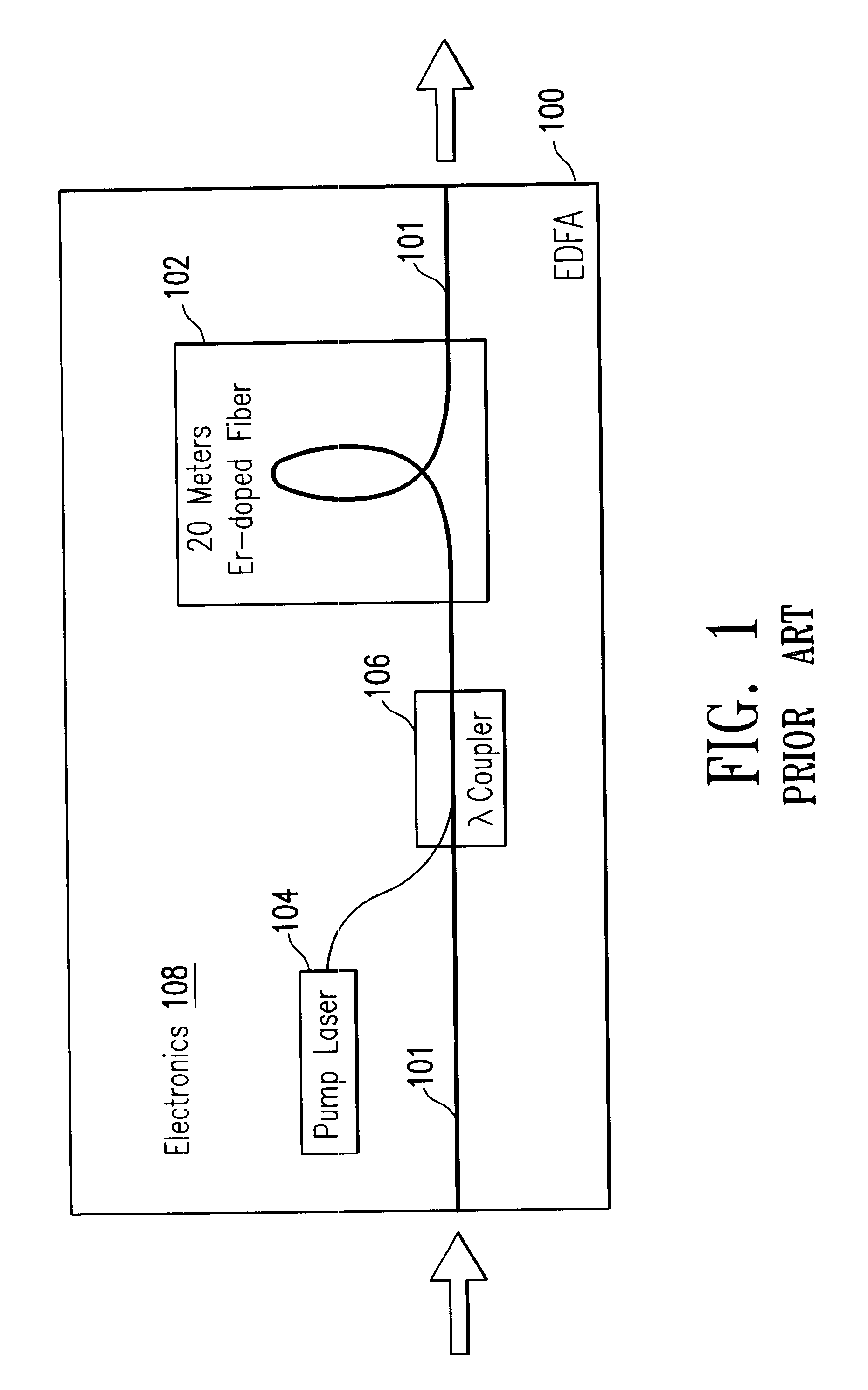
FIG. 1 is a schematic diagram of an erbium doped fiber amplifier (EDFA) 100. The EDFA 100 typically includes about 20 meters of erbium-doped fiber 102 inserted into the fiber optics. A pump laser 104 provides light to excite the ions in the erbium-doped fiber 102, and a wavelength coupler 106 couples the light from the pump laser 104 to the fiber optics 101. As discussed above, the EDFA 100 has its problems and disadvantages.

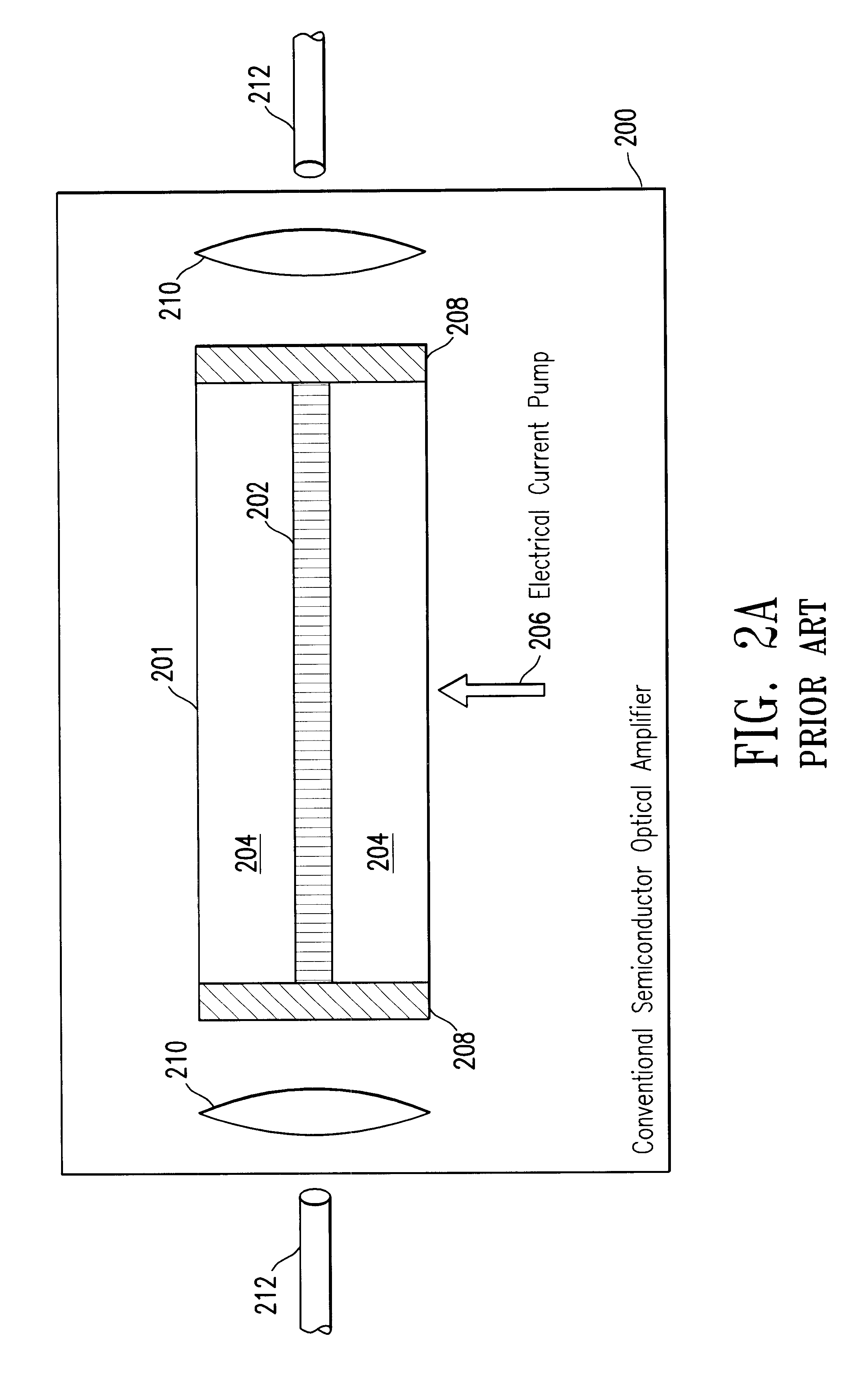
FIG. 2A is a schematic diagram of a conventional semiconductor optical amplifier (SOA) 200. The conventional SOA 200 comprises a semiconductor part 201 having an active region 202 with passive regions 204 surrounding the active region 202. The active region 202 comprises the semiconductor gain medium, and the passive regions 204 comprise wide bandgap semiconductor cladding regions. The edges of the semiconductor part 201 have antireflection coatings 208. The antireflection coatings 208 ensures that the semiconductor part 201 operates below a lasing threshold. Le...


PUM


Abstract

An optical signal power monitor and regulator comprises: a lasing semiconductor optical amplifier for receiving the optical signal and whose laser output is used to monitor a power level of the optical signal; a monitor circuit which receives the laser output and outputs a monitoring signal; a tunable element for receiving a version of the optical signal and whose level of amplification is adjustable and for outputting an amplified optical signal; and a regulator circuit for receiving the monitoring signal and adjusting the amplification of the tunable optical amplifier depending upon the monitoring signal. The tunable element may comprise a tunable gain-clamped semiconductor optical amplifier. Such an embodiment is capable of automatically regulating the tunable element such that a power level of the amplified optical signal is kept stable. In addition, the monitor circuit may be used to send status information regarding the optical signal to a network management system, which in turn may send to the regulator circuit a managing signal affecting the level of amplification to be applied to the optical signal.

Description

1. Field of the InventionThe present invention relates to optical communications systems. More particularly, the present invention relates to regulating and managing the operation of optical networks.2. Description of the Background ArtA. Optical Communications SystemsOptical communications systems are rapidly becoming a widespread and important technology in telecommunications and networking. Optical communications Systems transmit information optically at very high speeds over fiber optics.The basic components of an optical communications system include: an optical transmitter; fiber optics; and an optical receiver. An optical transmitter incorporates information to be communicated into an optical signal and sends the optical signal. Fiber optics carries the optical signal over a distance. Finally, the optical receiver receives the optical signal and recovers the information therein.B. Limited Dynamic Range of Optical ReceiversOne problem with optical communications systems relate...

Claims


Application Information

Patent Timeline
Patent Type & Authority Patents(United States)
IPC IPC(8): H01S5/00H01S5/183H01S5/50H01S5/062H01S5/028H01S5/14H01S5/0683
CPCH01S5/18302H01S5/0265H01S5/0285H01S5/0622H01S5/1021H01S5/1032H01S5/5072H01S5/18305H01S5/2027H01S5/4056H01S5/5027H01S5/142
Inventor DIJAILI, SOL P.WALKER, JEFFREY D.
Owner II VI DELAWARE INC
Why Eureka
Try Eureka