Method for manufacturing a micromechanical device

a micromechanical device and manufacturing method technology, applied in the field of micromechanical vibrating mirrors, can solve the problems of variable mirror properties, unpractical deep etching >100 .mu.m., and cost reasons

Inactive Publication Date: 2002-04-09
ROBERT BOSCH GMBH
View PDF16 Cites 67 Cited by
  • Summary
  • Abstract
  • Description
  • Claims
  • Application Information

AI Technical Summary

Problems solved by technology

In the case of surface-micromechanical concepts, the edge deflection is limited by the small substrate clearance of a few micrometers, while in the case of bulk-micromechanical components, the thick torsion-spring suspension mounts permit only relatively small torsion angles, even given large drive voltages, or manufacturing tolerances give rise to substantial variations in the mirror properties.
However, deep etching >100 .mu.m is not actually practical for reasons of cost.

Method used


Image

  • Method for manufacturing a micromechanical device
  • Method for manufacturing a micromechanical device
  • Method for manufacturing a micromechanical device

Examples


first embodiment

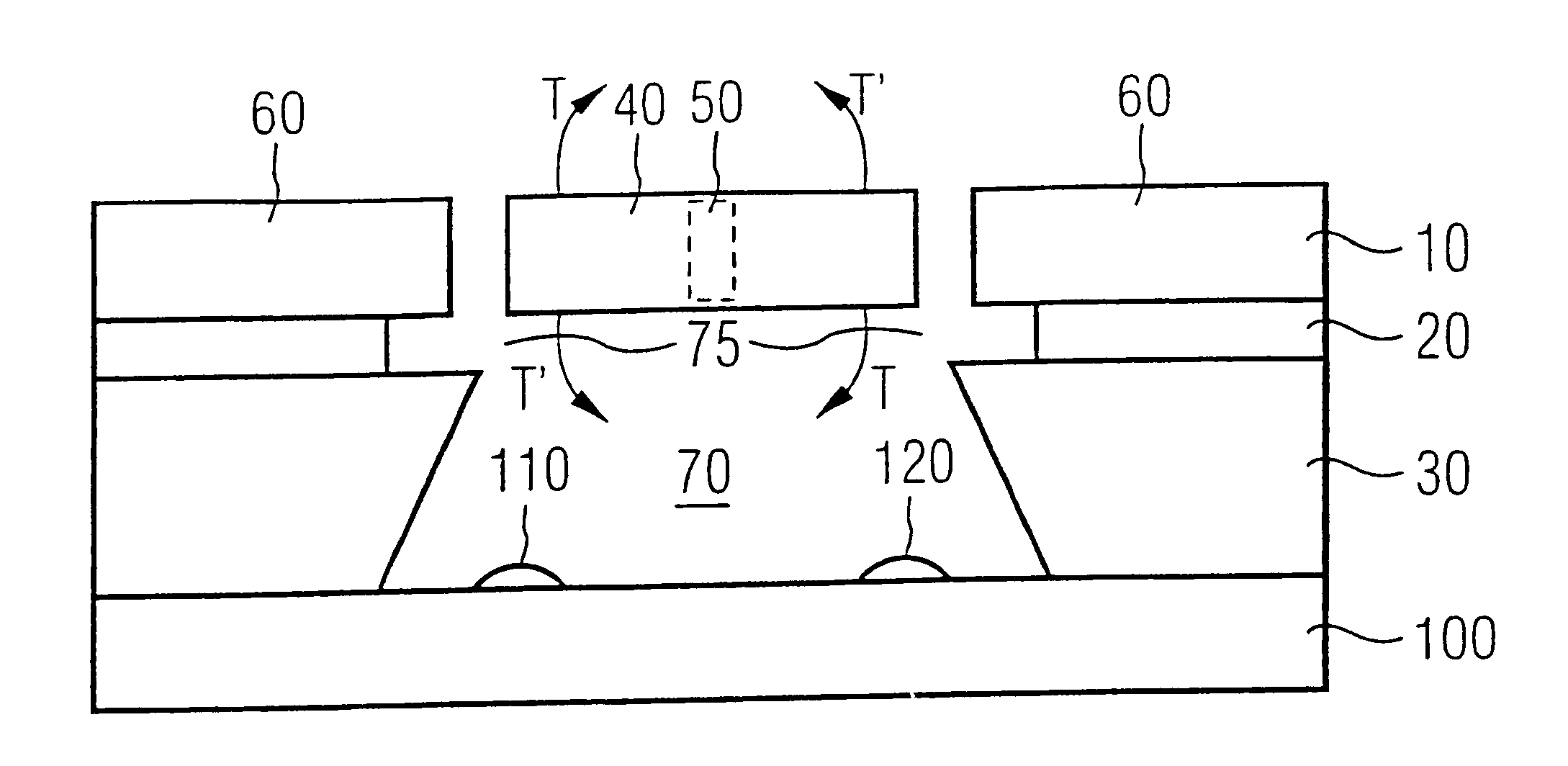
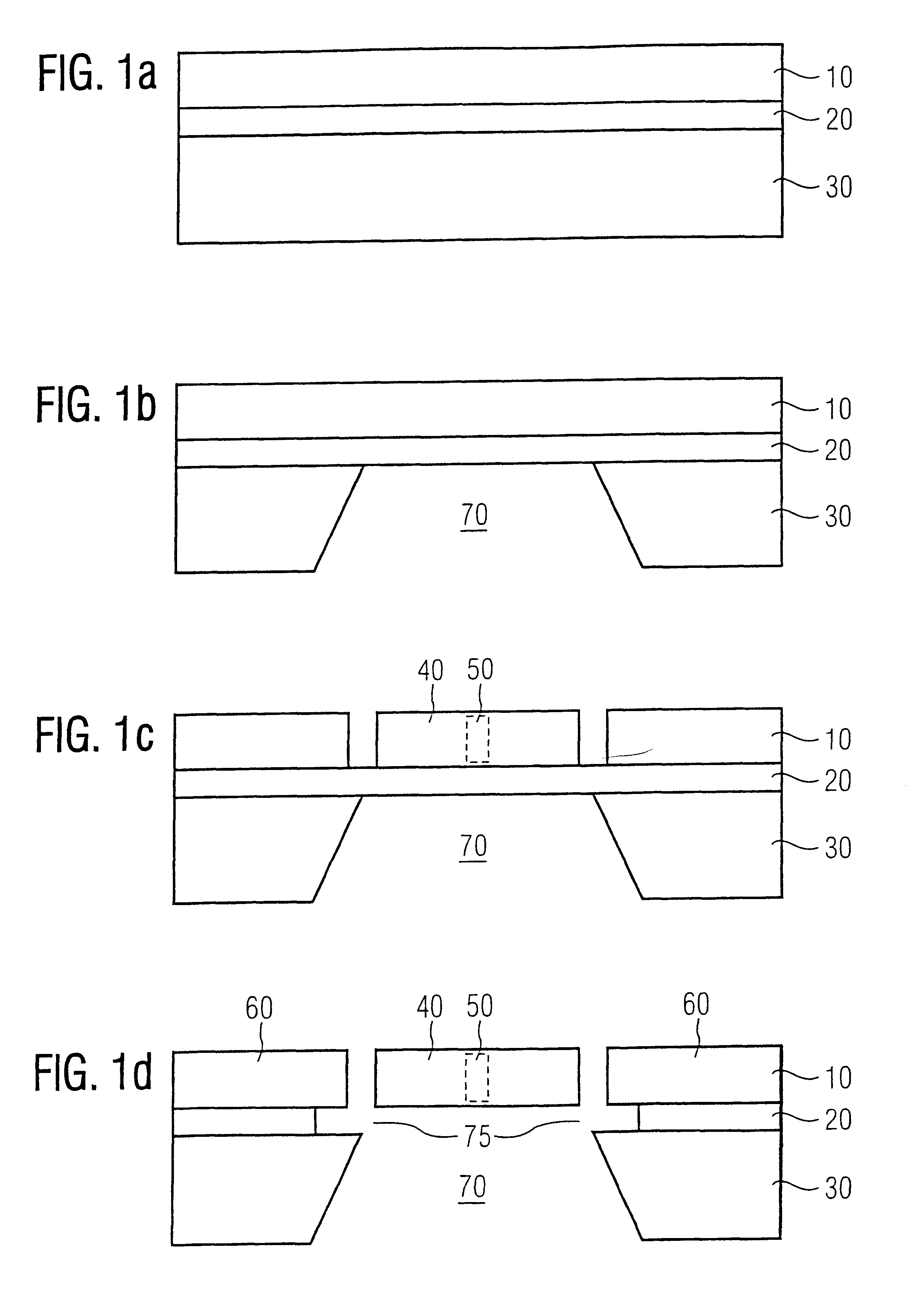
FIG. 1a-1e show a cross-sectional representation of the process steps according to the method of the present invention for manufacturing a vibrating mirror.

FIG. 1a shows an SOI wafer structure having an SOI layer 10 which is provided on a silicon substrate layer 30, with the interposition of an insulating layer 20 (e.g., an oxide layer).

According to FIG. 1b, silicon substrate layer 30 is etched through up to insulating layer 20 by wet etching. This is advantageously done with TMAH, KOH, and is carried out with an SOI wafer that is protected from etching on the front side and is masked on the back surface for producing a cavity region 70.

According to FIG. 1c, SOI layer 10 is thereupon etched through to insulating layer 20 to produce an island region 40, lying on insulating layer 20, which is joined to region 60 of SOI layer 10 surrounding island region 40 by way of two connecting webs 50 (see FIG. 3). The etching is carried out by a suitable dry-etching method such as plasma trenchin...

second embodiment

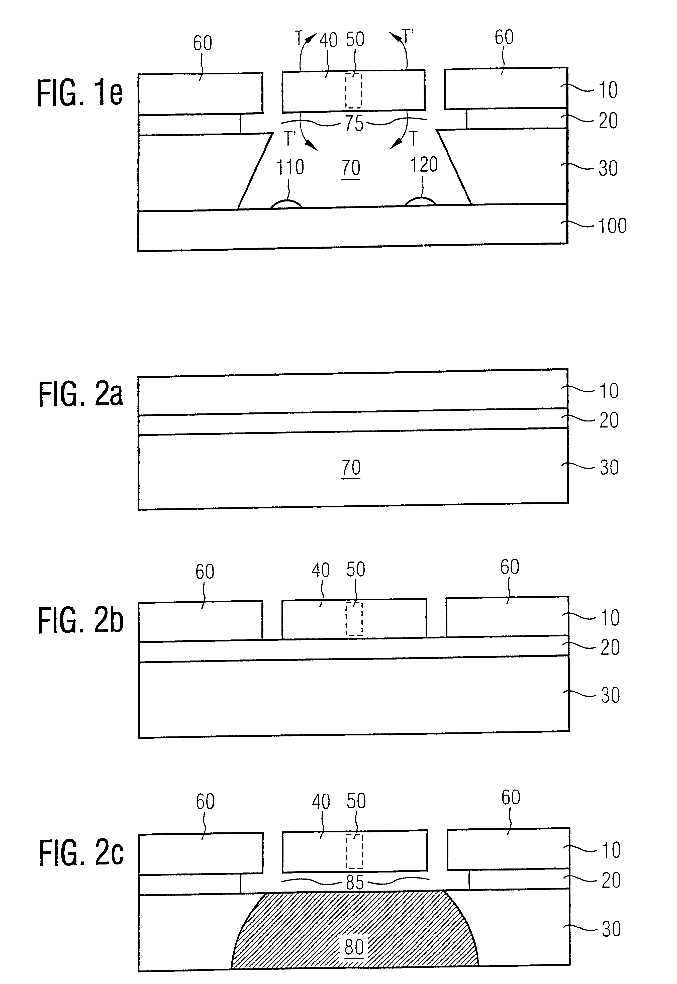
FIGS. 2a-2e show a cross-sectional representation of the process steps according to the method of the present invention for manufacturing a vibrating mirror.

FIG. 2a shows the same representation as FIG. 1a, thus a customary SOI structure.

In contrast to the first embodiment, according to FIG. 2b, first of all, SOI layer 10 is etched up to insulating layer 20 to produce island region 40 corresponding to the vibrating mirror which is joined by way of the two connecting webs 50 to region 60 of the first layer surrounding island region 40. This is done as in the first embodiment by a suitable dry etching method with high lateral resolution such as plasma trenching.

According to FIG. 2c, anodization is carried out when working with a back surface that is suitably masked with gold, for example, it being possible to detect an end point by a sudden voltage change in response to the complete anodization of the backside cavity region 80 to be formed. An electrolytic contacting of the highly dop...


PUM

PropertyMeasurementUnit
structureaaaaaaaaaa
anisotropicaaaaaaaaaa
metallicaaaaaaaaaa

Abstract

A method for manufacturing a micromechanical device, in particular a micromechanical vibrating-mirror device, having the following steps: making available a three-layer structure having a first layer, a second layer and a third layer, the second layer lying between the first and the third layers; etching through the first layer up to the second layer to produce an island region, lying on the second layer, which is joined to region of the first layer surrounding the island region by way of one or more connecting webs, and etching through a region of the third layer up to the second layer and removing a region of the second layer below the island region in such a way that the island region can perform movements, preferably torsional vibrations, about the one or more connecting webs, the torsional vibrations having such an amplitude that a part of the island region extends into the etched-through region of the third layer.

Description

The present invention relates to a manufacturing method for a micromechanical device, in particular for a micromechanical vibrating mirror.BACKGROUND INFORMATIONAlthough applicable to any micromechanical devices, the present invention and the objective underlying it are clarified with reference to a micromechanical vibrating mirror.Several design variations exist for micromechanical vibrating mirrors. For example, an aluminum membrane can be deflected by electrostatic forces, as is described in Texas Instruments, L. J. Hornbeck, Proc. Soc. Photo-Opt. Instrum. Eng. 1150 (1989) 86; J. Buhler et al. J. MEMS 6 (1997) 126.Several publications describe movable mirrors made of monocrystalline silicon (IBM, K. E. Petersen, IBM J. Res. Develop. 24 (1980) 631) or of polysilicon (CSEM, V. P. Jaecklin et al., Proc. IEEE Micro Electro Mech. System Workshop, FL, USA (1993) 124).The problem on which the present invention is based is that these concepts, above all in the case of large mirrors havin...

Claims


Application Information

Patent Timeline
Patent Type & Authority Patents(United States)
IPC IPC(8): B81B3/00G02B26/08
CPCB81B3/004G02B26/0841B81C1/00142B81B2201/0292B81C2201/019B81B2201/042
Inventor FUNK, KARSTENFREY, WILHELM
Owner ROBERT BOSCH GMBH
Why Eureka
Try Eureka