Pattern layout structure in substrate

a substrate and pattern technology, applied in semiconductor devices, semiconductor/solid-state device details, electrical devices, etc., can solve the problems of difficult control of the planarity of the copper foil layer on the top of the insulative layer, and affecting the quality of the substra

Inactive Publication Date: 2002-04-30
SILICONWARE PRECISION IND CO LTD
View PDF7 Cites 52 Cited by
  • Summary
  • Abstract
  • Description
  • Claims
  • Application Information

AI Technical Summary

Problems solved by technology

Since the insulative layer is formed by coating, the planarity of the copper foil layer on the top of the insulative layer is hard to be controlled.
The non-controllable planarity of the copper foil layer will affect the photolithographic and etching quality of the copper foil layer, thereby, will lower the quality of the substrate, and in the mean time, will make the subsequent packaging process more difficult.
Accordingly, the stress between layers becomes relatively large such that the manufacturing process of the substrate becomes relatively difficult.
Therefore, the fact that there is an obvious d

Method used


Image

  • Pattern layout structure in substrate
  • Pattern layout structure in substrate
  • Pattern layout structure in substrate

Examples


Embodiment Construction

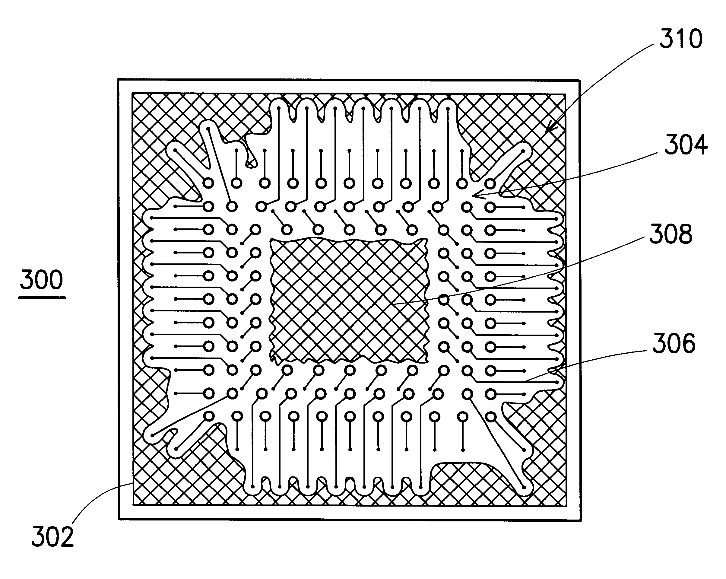
FIG. 3 is a cross-sectional view of a package substrate structure according to a preferred embodiment of the present invention. The preferred embodiment takes a built-up flip chip package having 4 layers as an example. That is, the patterned circuit layer constituted by a pair of copper foil layers positioned on each of the two sides of the insulative core layer and another pair of copper foil layers built up above and below the surfaces thereof respectively to become a 1+2+1 layer type of structure. As shown in FIG. 3, a package substrate 200 such as a flip chip BGA (Ball Grid Array) package of the preferred embodiment includes an insulative layers 202 made of "flame-retardant epoxy-glass fabric composite resin"(FR-4, FR-5) or Bismaleimide-Taiazine (BT) etc. A pair of patterned circuit layers 204 and 206 is formed on each of the two surfaces of the insulative core layer 202 respectively through the definition of photolithographic and etching process performing on a copper foil laye...


PUM


Abstract

A pattern layout structure of package substrate includes a plurality of patterned circuit layers alternately stacking up with at least an insulative layer for isolating the patterned circuit layers wherein the patterned circuit layers are electrically connected each other. The feature of the pattern layout is that the patterned circuit layer includes a signal circuit region, a power/ground region, and a dummy circuit region. The signal circuit region includes a multiplicity of conductive traces, and the power/ground region includes a first grid-like pattern while the dummy circuit region includes a second grid-like pattern. The pitch of either the first or second grid patterns is equal to the pitch of the conductive traces.

Description

1. Field of the InventionThis invention relates to a pattern layout structure in substrate, and more particularly to a pattern layout structure in substrate that makes use of grid dummy pattern structure to improve the planarity and quality of the built-up substrate.2. Description of Related ArtIn the course of the development of the IC package technology, since the integration of the semiconductor is increasing and the chip design gradually tends toward functional integration, a lot of SOC (System On Chip) products are produced one after another. As a result, following the enhancement of the data processing capability, the numbers of the I / O (input / output) terminals required by the chip are getting more and more, and the size of the chip is increasing. Accordingly, in recent years, the number of IC package product having high density and high pin (or lead) count is increasing day by day.Among the IC package products having high density and high pin (lead) count, the substrate type ...

Claims


Application Information

Patent Timeline
IPC IPC(8): H01L23/48H01L23/498
CPCH01L23/49838H01L23/4985H01L2924/0002H01L2924/00
Inventor TSAI, YING CHOU
Owner SILICONWARE PRECISION IND CO LTD
Why Eureka
Try Eureka