Transparent electrode based on metal nanometer grid and preparing method of transparent electrode

A metal nano and transparent electrode technology, which is applied in the manufacture of circuits, electrical components, semiconductors/solid-state devices, etc., can solve the problems of unsatisfactory large-scale production, high price, and poor uniformity, and achieve easy integration and large-scale production. Integrated and mass-produced, structurally shape-tunable effects

Inactive Publication Date: 2015-04-01
THE NAT CENT FOR NANOSCI & TECH NCNST OF CHINA
View PDF11 Cites 43 Cited by
  • Summary
  • Abstract
  • Description
  • Claims
  • Application Information

AI Technical Summary

Problems solved by technology

[0003] At present, indium tin oxide (ITO) transparent electrodes are widely used because of their good photoelectric properties, but traditional ITO transparent electrodes have exposed more and more problems: (1) The chemical and thermal properties of ITO are unstable; (2) ) In is a rare metal, expensive and toxic; (3) Compared with Ag, Ni and other metals, the high resistivity of ITO cannot meet the requirements of many devices for low resistivity; Low light transmittance limits its application; (5) The ITO thin film electrode prepared on a flexible substrate produces cracks when the substrate is bent, and the sheet resistance increases significantly with the number of bending times
The line width obtained by the self-assembly method is not easy to adjust, the uniformity is poor, and the efficiency is low, which cannot meet mass production

Method used


Image

  • Transparent electrode based on metal nanometer grid and preparing method of transparent electrode
  • Transparent electrode based on metal nanometer grid and preparing method of transparent electrode

Examples


Embodiment 1

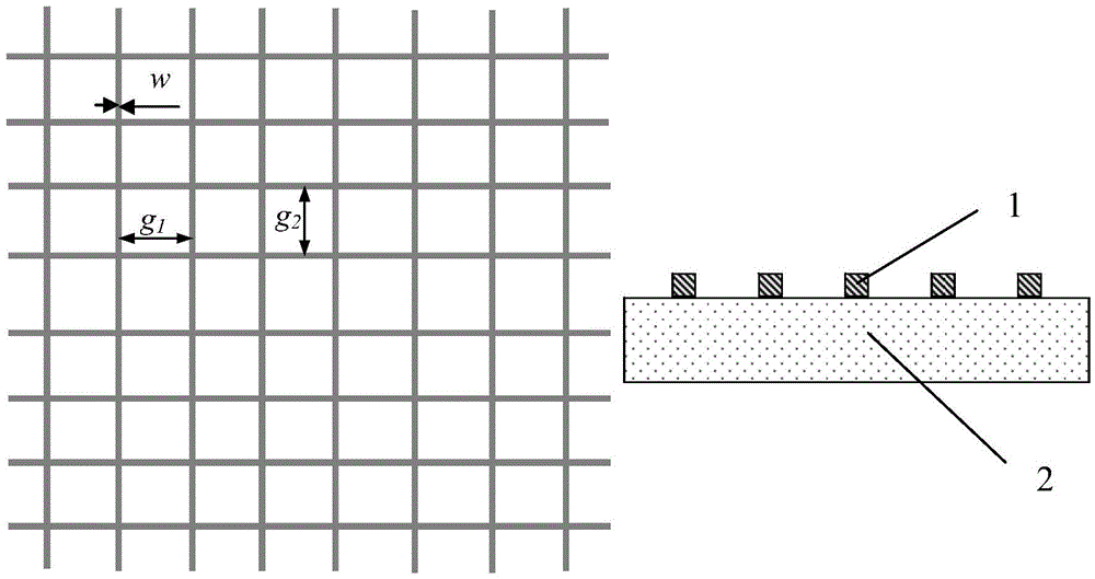
[0067] A transparent electrode based on a metal nanogrid is prepared by the following method:

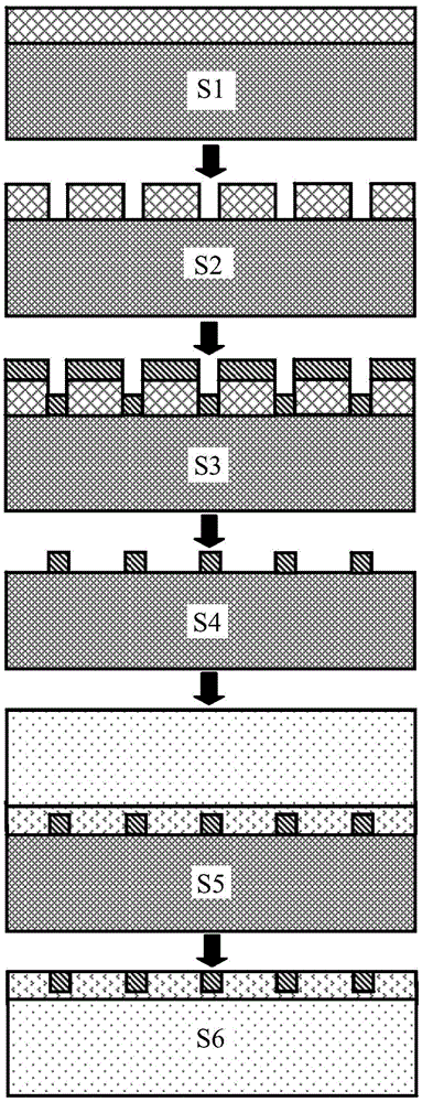
[0068] according to figure 2 Shown process flow diagram, described method comprises the following steps:

[0069] Step 1: Spin-coat photoresist on silicon substrate and bake;

[0070] In this step, bake the cleaned silicon substrate on a hot plate at 180°C for 5-10 minutes, remove the moisture on the surface, spin-coat PMMA (German Allresist company) electron beam positive photoresist, and place it on the hot plate Bake at 180°C for 2 minutes;

[0071] Step 2: Exposure and development, etching the photoresist to form nano-grid patterns on the silicon substrate;

[0072] In this step, the PMMA on the silicon substrate is exposed by electron beam direct writing technology, and a nano-grid pattern is formed on the photoresist layer after development; MIBK (methyl isobutyl ketone) with a mass ratio of 1:3 is used The mixed solution of IPA (isopropyl alcohol) is used as developing s...

Embodiment 2

[0083] A transparent electrode based on a metal nanogrid is prepared by the following method:

[0084] according to figure 2 Shown process flow diagram, described method comprises the following steps:

[0085] Step 1: Spin-coat photoresist on thinned silicon substrate and bake;

[0086] In this step, after the silicon substrate is thinned to 200 μm, it is cleaned, and then placed on a hot plate and baked at 180°C for 5-10 minutes to remove the moisture on the surface, and spin-coat PR1-500A (Futurrex product of the United States) electron beam positive photoresist, and placed on a hot plate to bake at 110°C for 5min;

[0087] Step 2: Exposure and development, etching the photoresist to form nano-grid patterns on the silicon substrate;

[0088] In this step, the PR1-500A on the silicon substrate is exposed by optical lithography using projection lithography equipment, and a nano-grid pattern is formed on the photoresist layer after development; use DR6 (Futurrex Company of ...

Embodiment 3

[0099] A transparent electrode based on a metal nanogrid is prepared by the following method:

[0100] according to figure 2 Shown process flow diagram, described method comprises the following steps:

[0101] Step 1: Spin-coat photoresist on thinned silicon substrate and bake;

[0102] In this step, after the silicon substrate is thinned to 150 μm, it is cleaned, and then placed on a hot plate and baked at 180 ° C for 5 to 10 minutes to remove the moisture on the surface, and spin-coat PMMA (Germany Allresist Company) electron beam positive Glue, and bake on a hot plate at 180°C for 5 minutes;

[0103] Step 2: Exposure and development, etching the photoresist to form nano-grid patterns on the silicon substrate;

[0104] In this step, the PMMA on the silicon substrate is exposed by electron beam direct writing technology, and a nano-grid pattern is formed on the photoresist layer after development; MIBK (methyl isobutyl ketone) with a mass ratio of 1:3 is used The mixed s...


PUM

PropertyMeasurementUnit
thicknessaaaaaaaaaa
thicknessaaaaaaaaaa
widthaaaaaaaaaa

Abstract

The invention relates to a preparing method of a transparent electrode based on a metal nanometer grid. The method comprises the following steps that (1) photoresist coats a silicon substrate in a spin-coating way and is baked; (2) exposure and development are carried out, and the photoresist is etched into a nanometer grid pattern on the silicon substrate; (3) a metal layer is deposited on the photoresist of the nanometer grid pattern; (4) the photoresist is removed through stripping, and a metal nanometer grid formed on the silicon substrate is obtained; (5) bonding agents coat the metal nanometer grid in a spin-coating way, and in addition, a transparent substrate is adhered and cured; (6) the silicon substrate is removed through corrosion, and the transparent electrode based on the metal nanometer grid arranged on the transparent substrate is obtained. The method is simple, the implementation is easy, the integration and the large-scale production are easily realized, and the electrical conductivity and the light transmittance of the prepared transparent electrode are controllable.

Description

technical field [0001] The invention relates to the field of electronic devices, in particular to a metal nanogrid-based transparent electrode and a preparation method thereof. Background technique [0002] A transparent electrode refers to a high light transmittance (above 85%) and low resistivity (1×10 -3 Ω cm below) characteristics of the electrode. Transparent electrodes are mainly used in flat display, solar cells, touch panels, electronic paper, transparent transistors and other fields. [0003] At present, indium tin oxide (ITO) transparent electrodes are widely used because of their good photoelectric properties, but traditional ITO transparent electrodes have exposed more and more problems: (1) The chemical and thermal properties of ITO are unstable; (2) ) In is a rare metal, expensive and toxic; (3) Compared with Ag, Ni and other metals, the high resistivity of ITO cannot meet the requirements of many devices for low resistivity; Low light transmittance limits i...

Claims


Application Information

Patent Timeline
Patent Type & Authority Applications(China)
IPC IPC(8): H01L21/28
CPCH01L21/28
Inventor 董凤良陈佩佩闫兰琴李志琴李志刚褚卫国
Owner THE NAT CENT FOR NANOSCI & TECH NCNST OF CHINA
Why Eureka
Try Eureka