Method for manufacturing semiconductor device, and laser irradiation apparatus

a laser irradiation and semiconductor technology, applied in the direction of transistors, chemistry apparatus and processes, crystal growth processes, etc., can solve the problems of difficult manufacturing of tft, difficult to form all channel-forming regions, and display unevenness visible to observer, so as to reduce adverse effects, reduce the variation in electrical characteristics of tft, and enhance the mobility of thin film transistors

Inactive Publication Date: 2007-07-24
SEMICON ENERGY LAB CO LTD
View PDF33 Cites 43 Cited by
  • Summary
  • Abstract
  • Description
  • Claims
  • Application Information

AI Technical Summary

Benefits of technology

[0041]The present invention can provide a crystalline semiconductor film in which the interval between the ridges, which is the size of the crystal grain, is controlled by irradiating once the pulsed laser whose polarization direction is controlled. Moreover, the orientation can be controlled by using the metal element for promoting the crystallization.
[0042]When such a crystalline semiconductor film is used to form the thin film transistor, it is possible to manufacture the thin film transistor having uniform electrical characteristic. In addition, the mobility of the thin film transistor can be enhanced by forming the channel-forming region so that the direction in which the current flows conforms to the direction in which the crystal grain is arranged.
[0043]Moreover, the interval between the ridges, which is the size of the crystal grain, is almost equal to the wavelength of the laser light to be irradiated, and it is extremely short. Therefore, since the channel-forming region has a plurality of crystal grains, it is possible to decrease the adverse affect in the crystal grain boundary and to reduce the variation in the electrical characteristic of TFT compared to the case where the number of crystal grains is small.

Problems solved by technology

However, the domain is formed at random and it is difficult to manufacture TFT so that the channel-forming region is formed within one domain.
Therefore, it becomes difficult to form all the channel-forming regions which are arranged in a pixel portion and a driver circuit portion respectively within one domain.
The variation in the electrical characteristic of TFT arranged in the pixel portion or the driver circuit portion causes the variation in the current and the voltage applied to each pixel electrode, which becomes the display unevenness that is visible for the observer.
In the future, however, when the pixel size is miniaturized further and the more precise image is demanded, this variation is considered to become a serious problem.
Therefore, there is a risk that a TFT having a boundary between the domains in the channel-forming region is formed.
The characteristic of such a TFT (mobility, S-value, on-current, off-current, and the like) varies compared with that of a TFT having a channel-forming region without any boundaries therein, and therefore this variation is considered to cause the display unevenness.
In such a crystallizing method, the process takes much time because the laser is irradiated to the silicon layer many times, for example 100 times.
In particular, when the crystalline semiconductor film formed by controlling the orientation with the use of a metal such as Ni is irradiated by the laser many times, it is impossible to maintain its orientation.
This means it takes much time to manufacture a semiconductor device or a thin film transistor, and therefore this method is unsuitable for mass production.

Method used


Image

  • Method for manufacturing semiconductor device, and laser irradiation apparatus
  • Method for manufacturing semiconductor device, and laser irradiation apparatus
  • Method for manufacturing semiconductor device, and laser irradiation apparatus

Examples


embodiment modes

(Embodiment Mode 1)

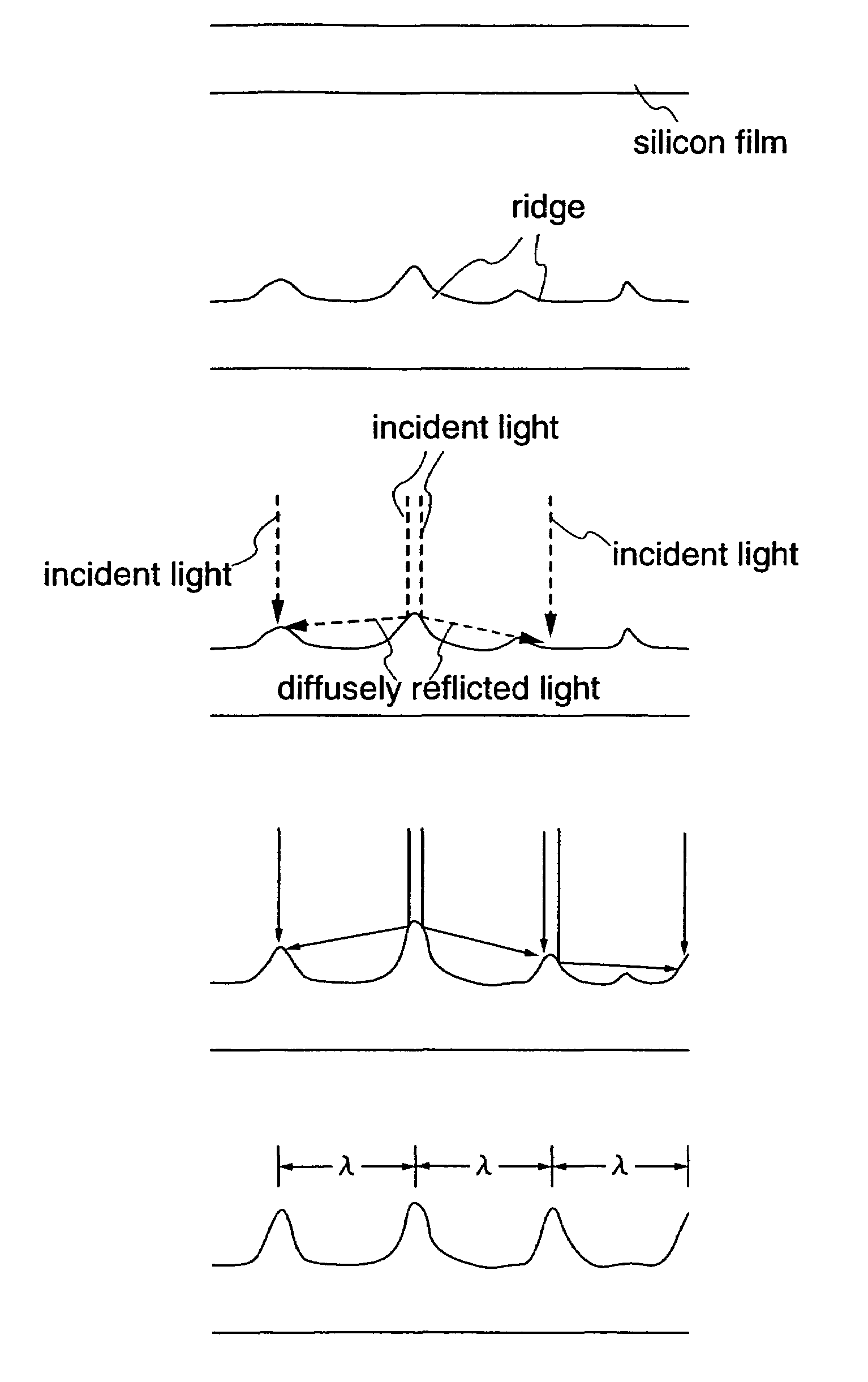
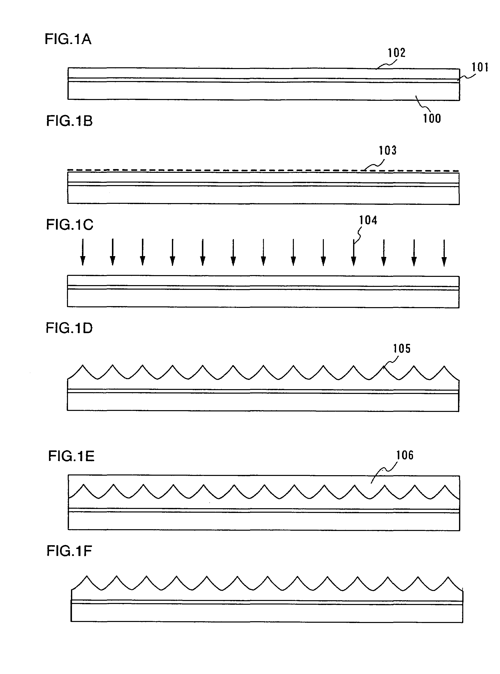
[0055]The present embodiment mode explains a method for manufacturing a crystalline semiconductor film in detail.

[0056]Initially, as shown in FIG. 1A, a base film 101 is formed on a substrate 100 having an insulating surface. A glass substrate such as a barium borosilicate glass or an alumino borosilicate glass, a quartz substrate, or an SUS substrate can be used as the substrate 100 for example. In addition, although a substrate made of flexible synthetic resin such as acryl or plastic typified by PET, PES, PEN, or the like tends to be inferior in resistance against the heat to the other substrates, the substrate made of flexible synthetic resin can be used when it can resist the heat generated in the manufacturing process.

[0057]The base film 101 is provided in order to prevent that alkali-earth metal or alkali metal such as Na included in the substrate 100 diffuses into the semiconductor film to have an adverse affect on a characteristic of a semiconductor devic...

embodiment mode 2

(Embodiment Mode 2)

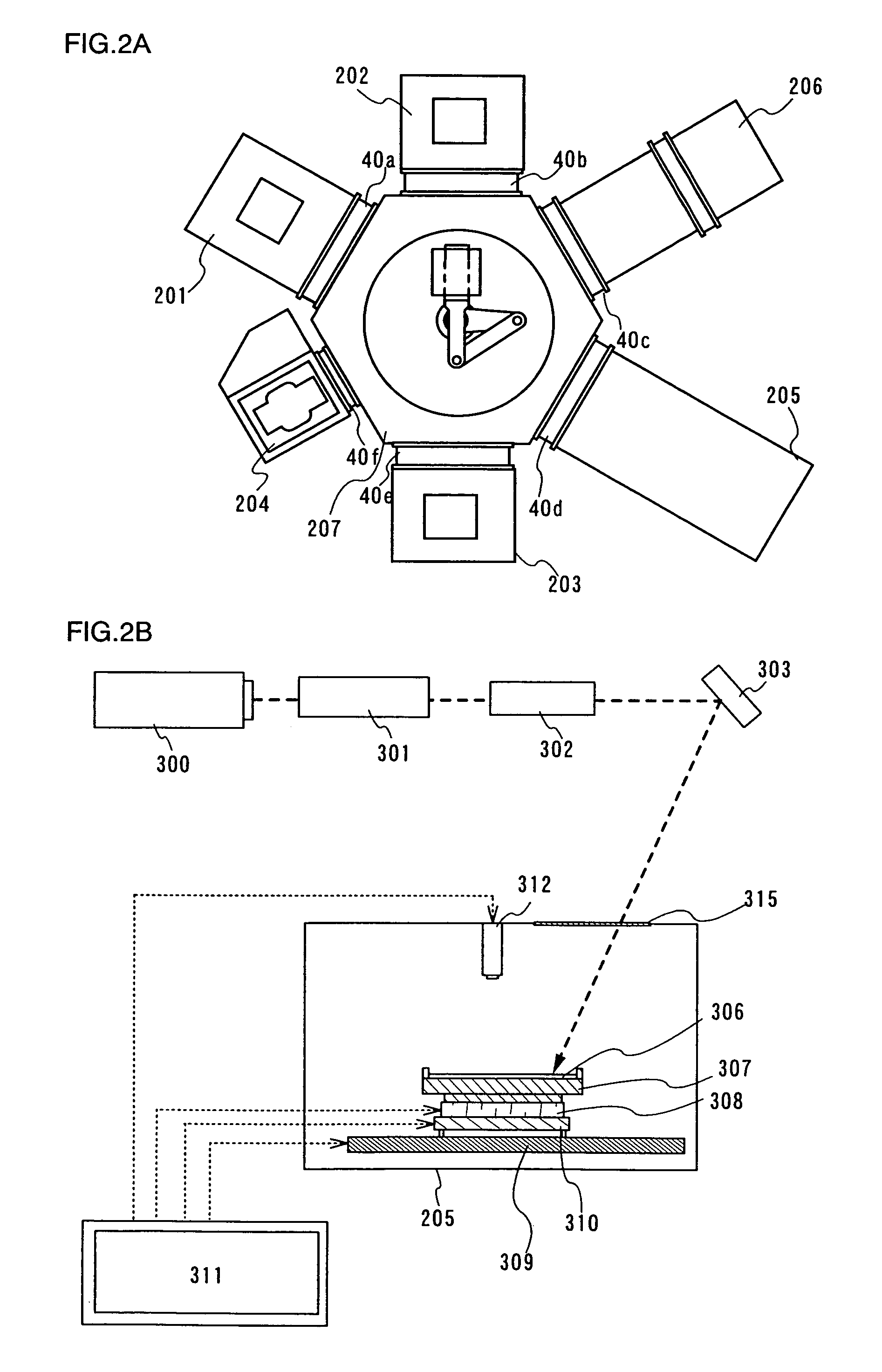
[0086]The present embodiment mode explains a multi-chamber apparatus having a laser irradiation apparatus and an optical system in the laser irradiation apparatus.

[0087]FIG. 2A shows a multi-chamber apparatus including a first treatment chamber 201 where the processes up to forming an amorphous semiconductor film can be performed, a second treatment chamber 202 where the metal element can be added, a third treatment chamber 203 where a heat treatment can be performed, an unload chamber 204 where a substrate can be unloaded, a laser irradiation chamber 205 where the laser irradiation is performed, and a load chamber 206 where the substrate can be stored, each of which is provided around a transferring chamber 207. Each treatment chamber and the like are connected to the transferring chamber 207 with transferring gates 40a to 40f respectively interposed therebetween. By providing each treatment chamber and the like around the transferring chamber having transferring...

embodiment mode 3

(Embodiment Mode 3)

[0106]The present embodiment mode explains a light-emitting device as an example of a semiconductor device having a crystalline semiconductor film.

[0107]FIG. 7A shows a light-emitting device where a signal line driver circuit 1200, a scanning line driver circuit 1201, and a pixel portion 1202 are formed on a first substrate 1210.

[0108]FIG. 7B is a cross-sectional view of the display device taken along A–A′ in FIG. 7A, which illustrates the signal line driver circuit 1200 equipped with a CMOS circuit having an n-channel TFT 1223 and a p-channel TFT 1224 on the first substrate 1210. The n-channel TFT 1223 and the p-channel TFT 1224 are formed using the crystalline semiconductor film of high quality obtained by performing the laser annealing with the use of the pulsed laser whose polarization direction is controlled. TFT forming the signal line driver circuit 1200 and the scanning line driver circuit 1201 may be formed by the CMOS circuit, a PMOS circuit, or an NMOS ...


PUM

PropertyMeasurementUnit
widthaaaaaaaaaa
angleaaaaaaaaaa
temperatureaaaaaaaaaa

Abstract

It is an object of the present invention to provide a method for manufacturing a crystalline semiconductor film comprising the steps of crystallizing with the use of the metal element for promoting the crystallization to control the orientation and irradiating the laser once to form a crystalline semiconductor film having a small crystal grain arranged in a grid pattern at a regular interval.In the present invention made in view of the above object, a ridge forms a grid pattern on a surface of the crystalline semiconductor film in such a way that a crystalline semiconductor film is formed by adding the metal element for promoting the crystallization to the amorphous semiconductor film and the pulsed laser whose polarization direction is controlled is irradiated thereto. As the means for controlling the polarization direction, a half-wave plate or a mirror is used.

Description

BACKGROUND OF THE INVENTION[0001]1. Field of the Invention[0002]The present invention relates to a crystalline semiconductor film having high crystallinity, to a thin film transistor having the crystalline semiconductor film, and to a semiconductor device having the thin film transistor. The present invention also relates to a crystallizing method for manufacturing the crystalline semiconductor film, the thin film transistor, and the semiconductor device. Furthermore, the present invention relates to a laser irradiation apparatus for providing the crystallizing method.[0003]2. Related Art[0004]Recently, a research has been advanced concerning a sophisticated semiconductor device using a thin film transistor. Particularly in the semiconductor device requiring rapidity and high functionality, it is necessary to obtain a thin film transistor (hereinafter also referred to as TFT) having high mobility.[0005]In order to enhance the crystallinity of the semiconductor film, the crystallizat...

Claims


Application Information

Patent Timeline
Patent Type & Authority Patents(United States)
IPC IPC(8): H01L21/00H01L21/84C30B13/24H01L21/20H01L21/77H01L29/04H01L29/786
CPCC30B13/24H01L21/2022H01L21/2026H01L27/1285H01L29/78675H01L27/1277H01L29/04H01L21/02686H01L21/02678H01L21/02502H01L21/02488H01L21/02532H01L21/02672H01L21/02595H01L21/02631H01L21/02691
Inventor SHIMOMURA, AKIHISAKOYAMA, MASAKISHOJI, HIRONOBU
Owner SEMICON ENERGY LAB CO LTD
Why Eureka
Try Eureka