Preparation apparatus for uniform silicon carbide crystals

a technology of silicon carbide crystals and preparation apparatuses, which is applied in the direction of crystal growth process, polycrystalline material growth, vacuum evaporation coating, etc., can solve the problems of material limitation, degradation of yield and quality, and the silicon seems to have reached its limit, so as to achieve uniform electrical characteristics

Active Publication Date: 2021-06-24
NAT CHUNG SHAN INST SCI & TECH
View PDF0 Cites 0 Cited by
  • Summary
  • Abstract
  • Description
  • Claims
  • Application Information

AI Technical Summary

Benefits of technology

[0007]It is therefore a primary objective of the present invention to provide a preparation apparatus for uniform silicon carbide crystals, to improve over disadvantages of the prior art. The present invention discloses a preparation apparatus for uniform silicon carbide crystals to stabilize and control the supply of dopants; the accessory does not participate in the reaction in the growth chamber but maintains its efficacy during growth. Finally, a single semi-insulating silicon carbide crystal with uniform electrical characteristics can be obtained.

Problems solved by technology

However, the development of silicon seems to have reached its limit, such that the growth of component performance is limited by the material.
However, rapid cooling at high temperatures is risky and may be accompanied by cracks and excessive internal stress in the crystal, causing degradation to yield and quality.
However, because vanadium is in direct contact with the silicon carbide source, a complex chemical reaction occurs between vanadium and the silicon carbide source at high temperatures, causing a variety of intermediate compounds such as vanadium carbide, silicon compounds, carbon-silicide, etc. and causing the doping of vanadium to be not uniform.
Although the gaseous dopant can stably control the doping dose, it generates byproduct halogen gas (Cl2) and hydrochloric acid (HCl), which pollute the environment, hurt human health, and impact mechanical maintenance.
The production materials are expensive and need a long time to grow.

Method used


Image

  • Preparation apparatus for uniform silicon carbide crystals
  • Preparation apparatus for uniform silicon carbide crystals
  • Preparation apparatus for uniform silicon carbide crystals

Examples


Embodiment Construction

[0024]The embodiments stated below are utilized for illustrating the concept of the present application. Those skilled in the art can easily understand the advantages and effects of the present invention disclosed by the application.

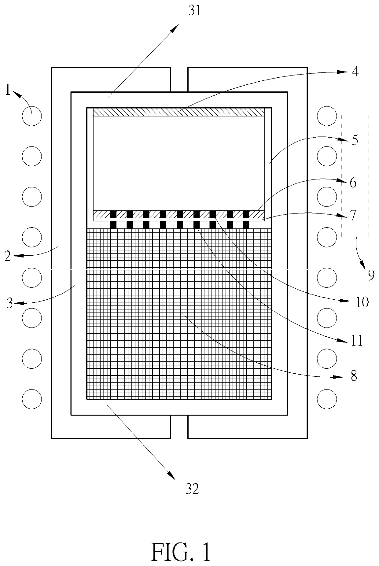
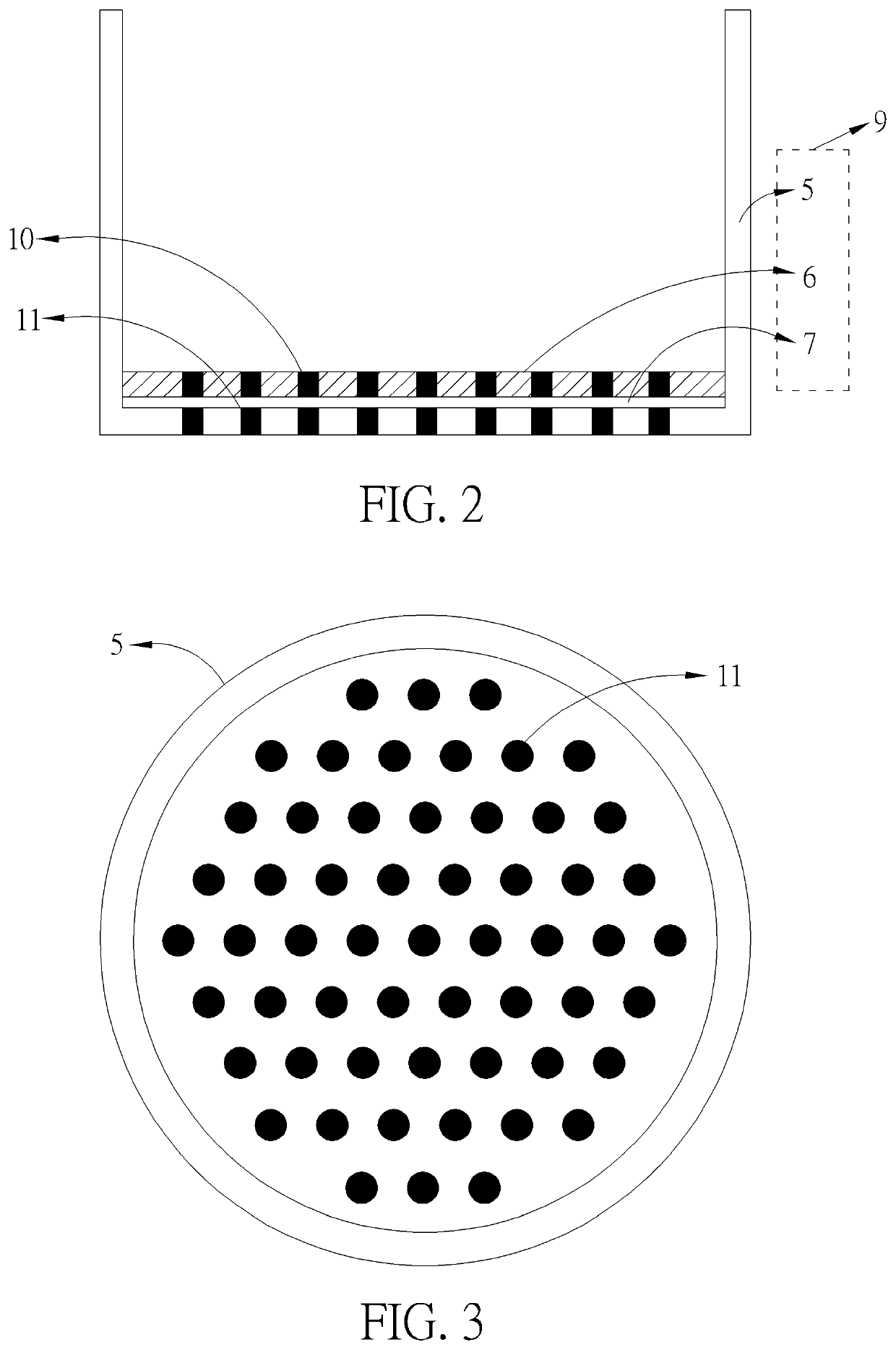
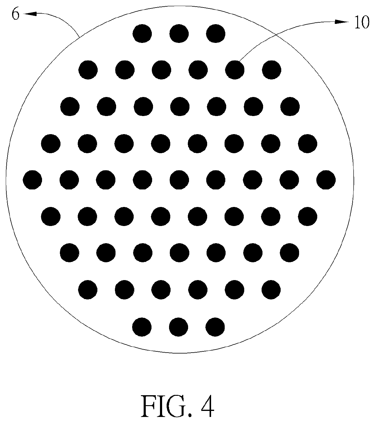
[0025]A physical vapor transport (PVT) method is utilized for the crystal growth of silicon carbide crystal, wherein the temperature for crystal growth is from 2000 to 2400° C., the pressure is 0.1-50 torr, and the growth rate generally falls to 100-250 μm / hr. The production materials are expensive and need a long time to grow. Therefore, it is important to increase yield; that is, it is necessary to stably produce a semi-insulating silicon carbide crystal with uniform electrical characteristics in fixed growth time. The present invention utilizes an internal accessory of graphite crucible to stabilize and control the supply of dopants; the accessory does not participate in the reaction in the growth chamber but maintains its efficacy during growth. Fina...


PUM

PropertyMeasurementUnit
pore diametersaaaaaaaaaa
thicknessaaaaaaaaaa
heightaaaaaaaaaa

Abstract

A preparation apparatus for uniform silicon carbide crystals comprises a circular cylinder, a doping tablet, and a plate to stabilize and control the supply of dopants. The accessory does not participate in the reaction in the growth chamber but maintains its efficacy during growth. Finally, a single semi-insulating silicon carbide crystal with uniform electrical characteristics can be obtained.

Description

BACKGROUND OF THE INVENTION1. Field of the Invention[0001]The present invention relates to a preparation apparatus for uniform silicon carbide crystals, and more particularly, to a preparation apparatus for uniform silicon carbide crystals applied to a graphite crucible.2. Description of the Prior Art[0002]With the development of technology, high power density, small components and high frequency operations have become essential. However, the development of silicon seems to have reached its limit, such that the growth of component performance is limited by the material. Thus, there is a need to develop new materials to replace the material currently used in the industry to break through the bottleneck. The excellent properties of silicon carbide can meet the specifications that cannot be reached by silicon currently. For example, the energy gap, the breakdown electric field, and the saturation electron drift rate of silicon carbide are 3, 10, and 2 times higher than traditional sili...

Claims


Application Information

Patent Timeline
Patent Type & Authority Applications(United States)
IPC IPC(8): C30B23/00C30B23/02C30B29/36C23C14/06C23C14/24
CPCC30B23/005C30B23/02C23C14/243C23C14/0635C30B29/36C30B35/002
Inventor KUO, CHIH-WEIMA, DAI-LIANGTAI, CHIA-HUNGYU, BANG-YINGKO, CHENG-JUNGLIN, BO-CHENGCHEN, HSUEH-I
Owner NAT CHUNG SHAN INST SCI & TECH
Why Eureka
Try Eureka