High density interconnect module

a high-density, interconnect module technology, applied in the direction of basic electric elements, electrical apparatus construction details, solid-state devices, etc., can solve the problems of increasing the cost of circuits, limited space along one-dimensional edges of integrated circuit chips, and increasing the size of the system

Inactive Publication Date: 2002-05-28
RAYTHEON CO
View PDF15 Cites 37 Cited by
  • Summary
  • Abstract
  • Description
  • Claims
  • Application Information

AI Technical Summary

Problems solved by technology

However, space is limited along the one-dimensional edges of integrated circuit chips.
The requirement for peripheral connections places design constraints on the integrated circuits, which may increase the cost of the circuits.
In addition, in systems requiring multiple interconnected integrated circuit chips, the use of peripheral connections often dramatically increases the space required to accommodate the multiple chips, thereby increasing the size of the system.
This is particularly problematic in applications such as cellular telephones and calculators where small circuit sizes are of paramount importance.
For example, the BGA substrates often have low thermal conductivity.
The low thermal conductivity decreases connection reliability due to differences in coefficients of thermal expansion between materials used for the balls and the integrated circuit contacts.
The packaging systems often lack adaptability features that allow removal of integrated circuits and replacement with new integrated circuits with different contact patterns.
As a result, the entire package is often discarded.
In addition, due to design limitations inherent in a conventional BGA system, the packaging systems often have unnecessarily large footprints to minimize cross-talk between connections and accommodate high frequency operation.

Method used


Image

  • High density interconnect module
  • High density interconnect module

Examples


Embodiment Construction

While the present invention is described herein with reference to illustrative embodiments for particular applications, it should be understood that the invention is not limited thereto. Those having ordinary skill in the art and access to the teachings provided herein will recognize additional modifications, applications, and embodiments within the scope thereof and additional fields in which the present invention would be of significant utility.

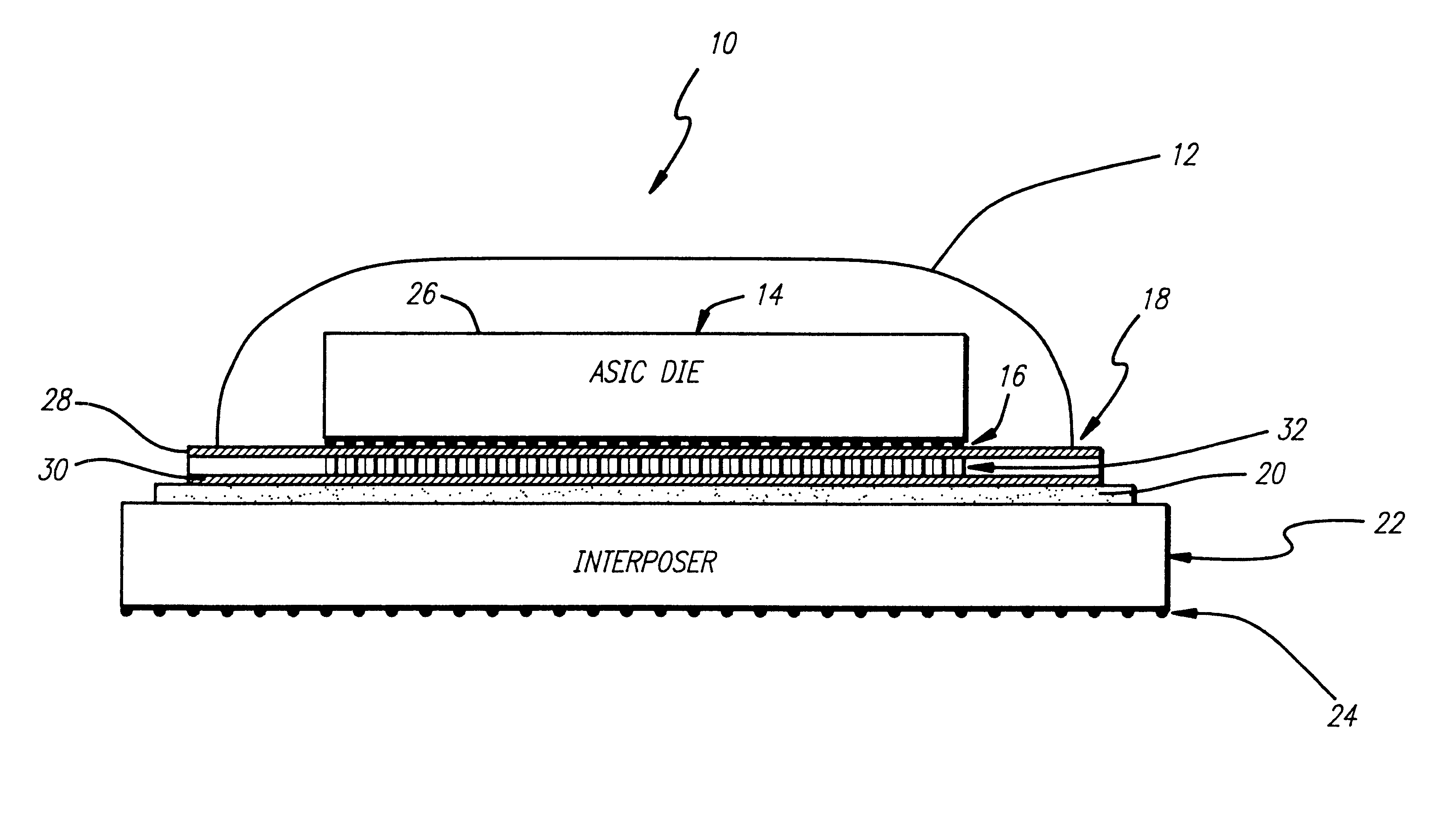
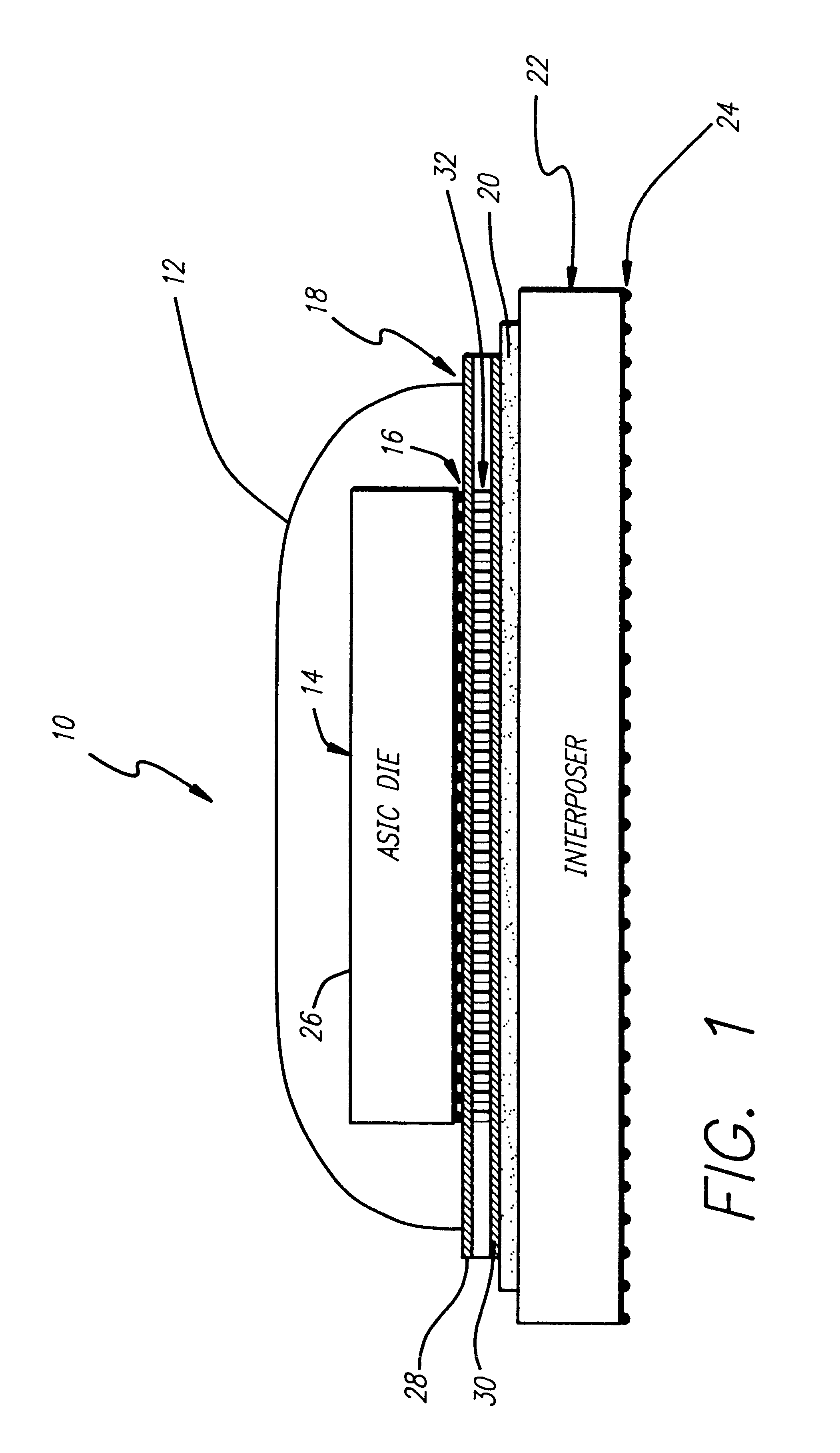
FIG. 1 is a diagram of a packaging system 10 constructed in accordance with the teachings of the present invention. The packaging system 10 includes, from top to bottom, an encapsulant sealer 12, an application specific integrated circuit (ASIC) die or chip 14, a first array of input / output contacts 16, a double-sided DECAL 18, a z-axis adhesive 20, an interposer 22, and a second array of input / output contacts 24.

The encapsulant sealer 12 is a non-non-hermetic and is made of plastic in the present specific embodiment. The ASIC die 14 is an ...


PUM


Abstract

A cost-effective packaging system (10) for ultra high density input/output (integrated circuits (14). The packaging system includes a first circuit chip (14) that has a first pattern of contacts (16) distributed across a surface area of the chip (14). The first pattern of contacts (16) represents input/output connections (16). A three-dimensional circuit (18) is disposed spatially parallel with respect to the first circuit chip (14) and organizes the input/output connections (16) into a second pattern of contacts (24, 30) suitable for connection to a second circuit (22). In a specific embodiment, the three-dimensional circuit (18) is a double sided DECAL (18). The double-sided DECAL (18) includes a substrate (18) having a first circuit pattern (28) spatially parallel with a second circuit pattern (30) on or in the substrate (18). The first and second circuit patterns (28 and 30) are interconnected. The first circuit pattern (28) has a third pattern of contacts (16) coincident with the first pattern of contacts (16) on the first circuit chip (14). The first circuit pattern (28) and/or the second circuit pattern (30) are ball grid arrays or coaxial connector arrays. The second circuit (22) is disposed spatially parallel with respect to the three-dimensional circuit (18). The second circuit (22) is a ceramic or laminate interposer that facilitates further organization of the input/output connections (16, 24). The interposer (18) includes a ball grid array (24) or a coaxial connector grid array (18) to facilitate the organization. A z-axis adhesive (20) is disposed between the interposer (22) and the three-dimensional circuit (18). A non-hermetic sealer (12) disposed over the first circuit chip (14).

Description

1. Field of InventionThis invention relates to electronic packaging. Specifically, the present invention relates to systems and methods for packaging microprocessors with highdensity input / output connections in space limited applications.2. Description of the Related ArtIntegrated circuits having hundreds or thousands of input / output connections are used in a variety of demanding applications ranging from computer chips to telecommunications digital signal processors. Such applications typically require cost-effective and reliable integrated circuit packaging systems that can effectively accommodate large numbers of interconnections between integrated circuits or circuit boards. Efficient electronic packaging systems and methods for packaging integrated circuit chips are becoming increasingly important as integrated circuits become smaller and more complex.A typical integrated circuit requires multiple input / output lines including power, ground, and signal lines. The lines are often...

Claims


Application Information

Patent Timeline
Patent Type & Authority Patents(United States)
IPC IPC(8): H01L23/48H01L23/498
CPCH01L23/49827H01L23/49838H01L2924/15311H01L2224/16H01L2924/00014H01L2224/0401
Inventor IWAMI, CRAIGHALL, JIM K.MULHOLLAND, BRIAN R.GREINER, SETH
Owner RAYTHEON CO
Why Eureka
Try Eureka