Method for making an insulating film

a technology of insulating film and film layer, which is applied in the direction of semiconductor devices, semiconductor/solid-state device details, electrical equipment, etc., can solve problems such as metal wiring corrosion

Inactive Publication Date: 2002-08-06
SONY CORP
View PDF12 Cites 15 Cited by
  • Summary
  • Abstract
  • Description
  • Claims
  • Application Information

AI Technical Summary

Benefits of technology

It is therefore an object of the invention to provide a method for making an insulating film free from problems such as corrosion of metal wiring and poisoned via even when a fluid source material is used to make the insulating film.
According to the invention, having the above-summarized construction configured to execute plasma processing, rapid thermal annealing by using lamp heating or ozone processing after making a first insulating film having a fluidity, H.sub.2 O can be removed from the surface of the first insulating film due to dehydrated condensation, and the film can be hardened. Therefore, even when NH.sub.3 is produced in the vapor by plasma while a SiO.sub.2 film is stacked on the first insulating film by plasma CVD using SiH.sub.4 and N.sub.2 O as the source material gases, NH.sub.3 can be prevented from being incorporated into the first insulating film. As a result, corrosion of metal wiring or the problem of poisoned via can be prevented.

Problems solved by technology

Under the condition, if the inter-layer insulating film underlying the SiO.sub.2 film contains H.sub.2 O and has a fluidity, then NH.sub.3 produced in the vapor is incorporated (absorbed) into the underlying inter-layer insulating film. NH.sub.3 incorporated into the underlying inter-layer insulating film is released from the film when the inter-layer insulating film is heated or etched in a later process, and probably cause the problems of corrosion of metal wiring and the poisoned via.

Method used


Image

  • Method for making an insulating film
  • Method for making an insulating film
  • Method for making an insulating film

Examples


first embodiment

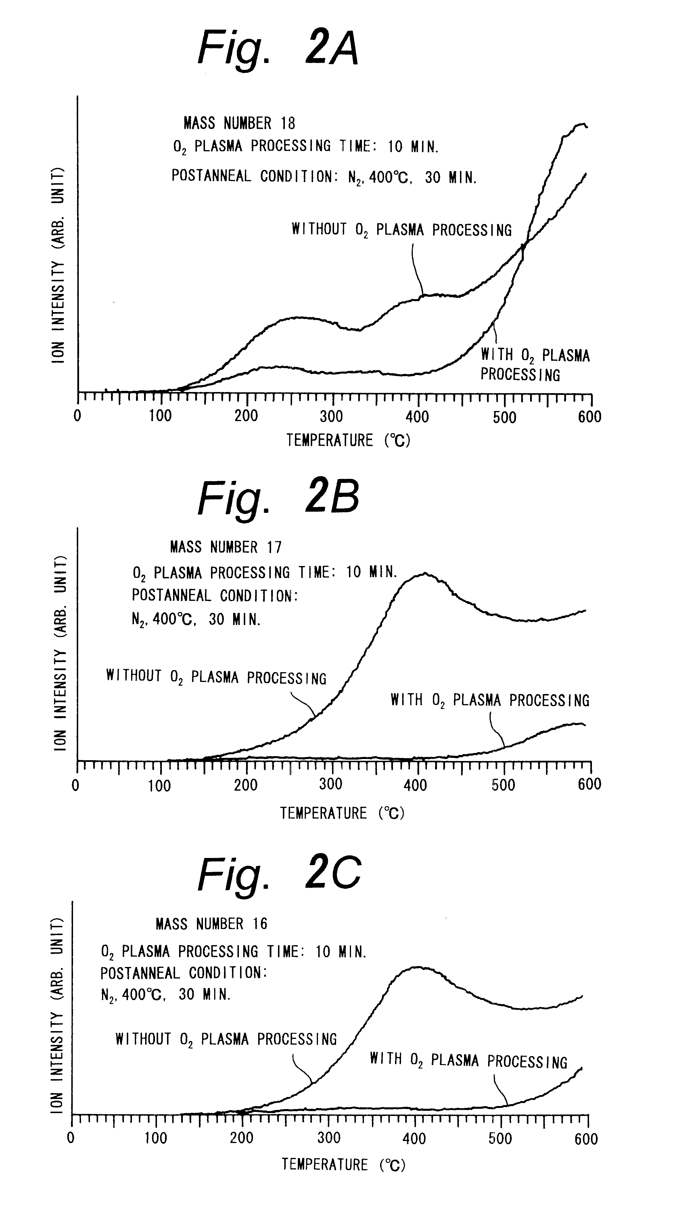
As explained above, substantially all H.sub.2 O can be removed from the surface of the inter-layer insulating film 4 by treating the inter-layer insulating film 4 by O.sub.2 plasma processing after making the inter-layer insulating film 4 as a fluid film. Therefore, even when the SiO.sub.2 film 5 is made as a cap layer directly on the inter-layer insulating film 4 by plasma CVD, NH.sub.3 produced in the vapor by the plasma during the process is never incorporated into the inter-layer insulating film 4. As a result, corrosion of the Al alloy wiring 2 or the problem of poisoned via do not occur.

second embodiment

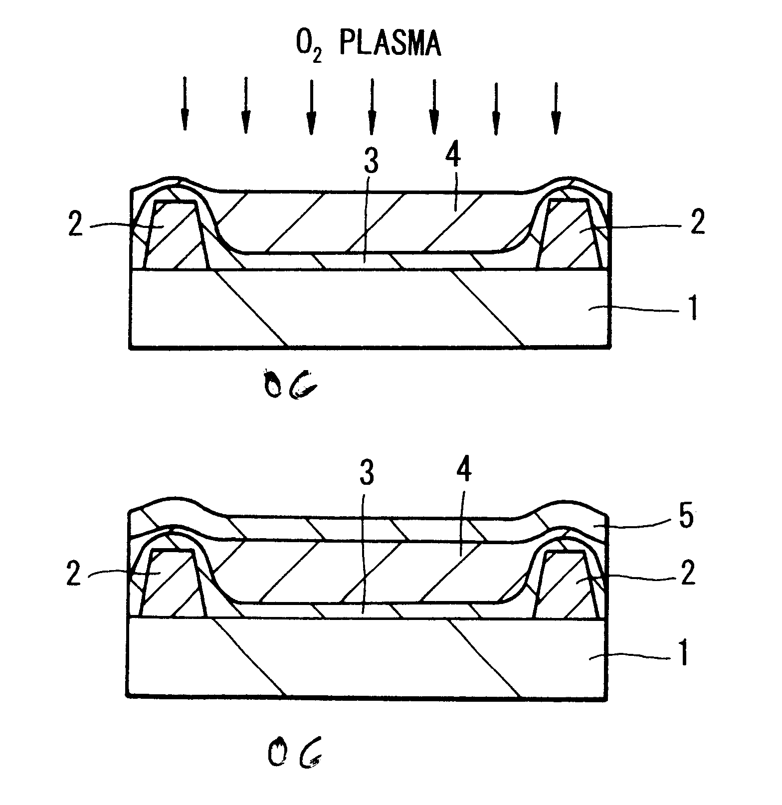
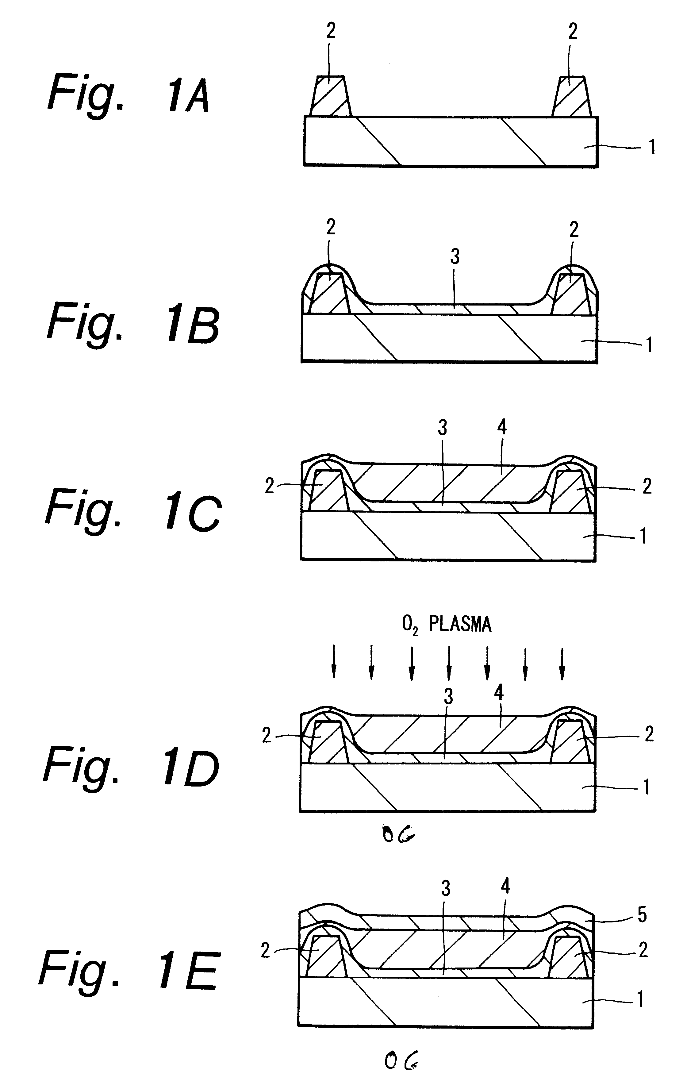
FIGS. 3A through 3E show a method for making an inter-layer insulating film according to the invention.

In the embodiment shown here, the Al alloy wiring 2 is formed on the Si substrate 1 having formed a device and covered with an inter-layer insulating film previously as shown in FIG. 3A,.

Next, as shown in FIG. 3B, a non-fluid SiO.sub.2 film 3 is made as a base layer on the Si substrate 1 by plasma CVD using SiH.sub.4 and N.sub.2 O, for example, as the source materials.

Next, as shown in FIG. 3C, a fluid inter-layer insulating film 4 is made by low pressure CVD using Si(CH.sub.3)H.sub.3 and H.sub.2 O.sub.2, for example, as the source materials. The steps heretofore are the same as those of the first embodiment.

Next, as shown in FIG. 3D, the surface of the inter-layer insulating film 4 is heated by lamp heating, namely by using radiant heat from a lamp heater, to cure the surface of the inter-layer insulating film 4 by rapid thermal annealing in a short time. By the rapid thermal anne...

third embodiment

FIGS. 4A through 4E show a method for making an inter-layer insulating film according to the invention.

In the embodiment shown here, the Al alloy wiring 2 is formed on the Si substrate 1 having formed a device and covered with an inter-layer insulating film previously as shown in FIG. 4A.

Next, as shown in FIG. 4B, a non-fluid SiO.sub.2 film 3 is made as a base layer on the Si substrate 1 by plasma CVD using SiH.sub.4 and N.sub.2 O, for example, as the source materials.

Next, as shown in FIG. 4C, a fluid inter-layer insulating film 4 is made by low pressure CVD using Si(CH.sub.3)H.sub.3 and H.sub.2 O.sub.2, for example, as the source materials. The steps heretofore are the same as those of the first embodiment.

Next, as shown in FIG. 4D, the Si substrate 1 is set in a chamber 6 and heated while introducing O.sub.3 into the chamber to cure the surface of the inter-layer insulating film 4 by O.sub.3 annealing of the inter-layer insulating film 4. By the O.sub.3 annealing, dehydrated cond...


PUM

PropertyMeasurementUnit
temperatureaaaaaaaaaa
heightaaaaaaaaaa
heightaaaaaaaaaa

Abstract

In a method for manufacturing an insulating film using a fluid source material without inviting corrosion of metal wiring or the problem of poisoned via, after making a SiO2 film as a base layer on an Si substrate defining an uneven surface with an Al alloy wiring by plasma CVD using SiH4 and N2O, and further making an inter-layer insualting film having a fluidity on the SiO2 film by low pressure CVD using SiH4 or organosilane and H2O2, O2 plasma processing is applied to the inter-layer insulating film. After that, a SiO2 film as a cap layer is made on the inter-layer insulating film by plasma CVD using SiH4 and N2O. Rapid thermal annealing using lamp heating or O3 annealing may be done in lieu of O2 plasma processing.

Description

1. Field of the InventionThis invention relates to a method for making an insulating film particularly suitable for use in making an inter-layer insulating film in a semiconductor device.2. Description of the Related ArtIn a process of manufacturing a semiconductor device, a method for making an inter-layer insulating film using a fluid source material is often used to level the surface of a substrate by smoothing unevenness made by wiring or the like. Such an inter-layer insulating film contains much moisture (H.sub.2 O) and is highly fluid.In conventional techniques, a non-fluid cap layer was formed directly on a fluid inter-layer insulating film containing much H.sub.2 O by plasma CVD (for example, 1995 Dry Process Symposium, pp.261-268) to prevent cracks in the fluid inter-layer insulating film containing H.sub.2 O during post-annealing. Typically used as the cap layer was a SiO.sub.2 film made of SiH.sub.4 and N.sub.2 O by plasma CVD because N.sub.2 O was more preferable than O...

Claims


Application Information

Patent Timeline
Patent Type & Authority Patents(United States)
IPC IPC(8): H01L21/768H01L21/70H01L21/316H01L23/522
CPCH01L21/76801H01L21/76826H01L21/76828H01L21/76834H01L21/31
Inventor HARA, MASAKI
Owner SONY CORP
Why Eureka
Try Eureka