Signal processing circuit for charge generation type detection device

a signal processing circuit and detection device technology, applied in the field of signal processing circuits, can solve the problems of large error in the output voltage of large high-frequency noise the infrared radiation detection circuit having a wide dynamic range, so as to reduce the dc offset error in the output voltage, reduce the noise of the 1/f, and reduce the noise of the output voltag

Inactive Publication Date: 2002-08-06
PANASONIC CORP
View PDF11 Cites 5 Cited by
  • Summary
  • Abstract
  • Description
  • Claims
  • Application Information

AI Technical Summary

Benefits of technology

Thus, the invention described herein makes possible the advantages of: (1) providing a signal processing circuit for a charge generation type detection device having a reduced DC offset error in the output voltage and reduced high-frequency noise to the output voltage; (2) providing a signal processing circuit for a charge generation typ

Problems solved by technology

The error has been A significant drawback to realization of high-sensitivity infrared radiation detection.
The high-frequency noise has been a significant drawback to realization of high-sensitivity infrared radiation detection.
This has been a drawback to realization of an infrared radiation detection circuit having a wide dynamic range.
This increases the circuit scale of the infrared radiation detection apparatus, thereby making the apparatus high in cost and large in size.
In addition, external noise, particularly a 50 Hz or 60 Hz commercial frequency, may further be superimposed on the output voltage V.sub.o, thereby reducing the infrared radiation detection capability.
Howeve

Method used


Image

  • Signal processing circuit for charge generation type detection device
  • Signal processing circuit for charge generation type detection device
  • Signal processing circuit for charge generation type detection device

Examples


embodiment 1

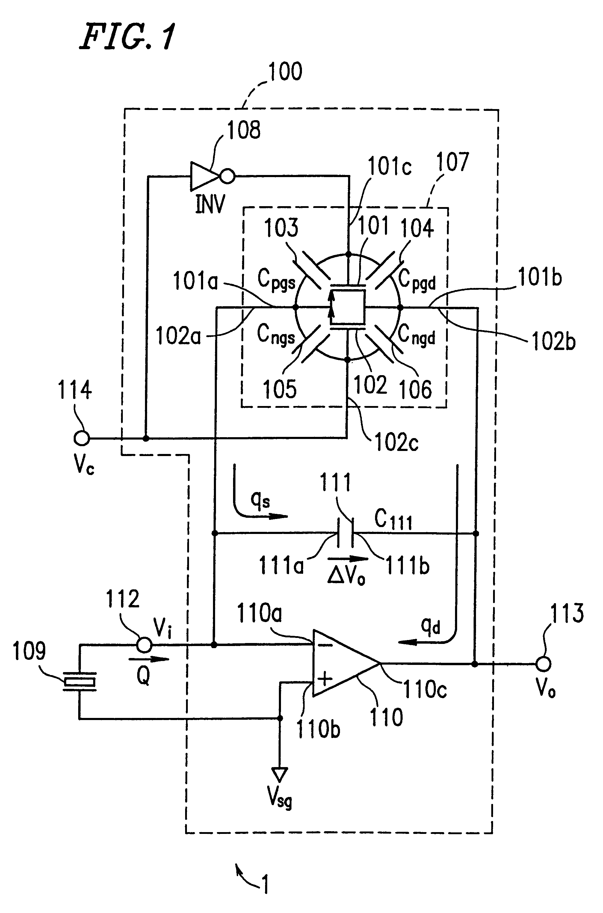
illustrates an example where the CMOS type switch 107 is used as the reset switch of the charge-voltage conversion circuit 100. However, the reset switch of the charge-voltage conversion circuit 100 is not limited to a CMOS type switch. For example, the reset switch of the charge-voltage conversion circuit 100 may alternatively be a switch including a first transistor (either P-type or N-type) for generating a clock feed-through and A second compensation transistor (either P-type or N-type regardless of the conductivity type of the first transistor) for absorbing the clock feed-through generated by the first transistor. When a CMOS type switch is used as the reset switch of the charge-voltage conversion circuit 100, the first translator has a conductivity type different from that of the second transistor.

Each of the above-described modifications to the switch 107 may also be used in any of the other embodiments which Will be described below with reference to FIGS. 2, 3, 5 to 7.

embodiment 2

(Embodiment 2)

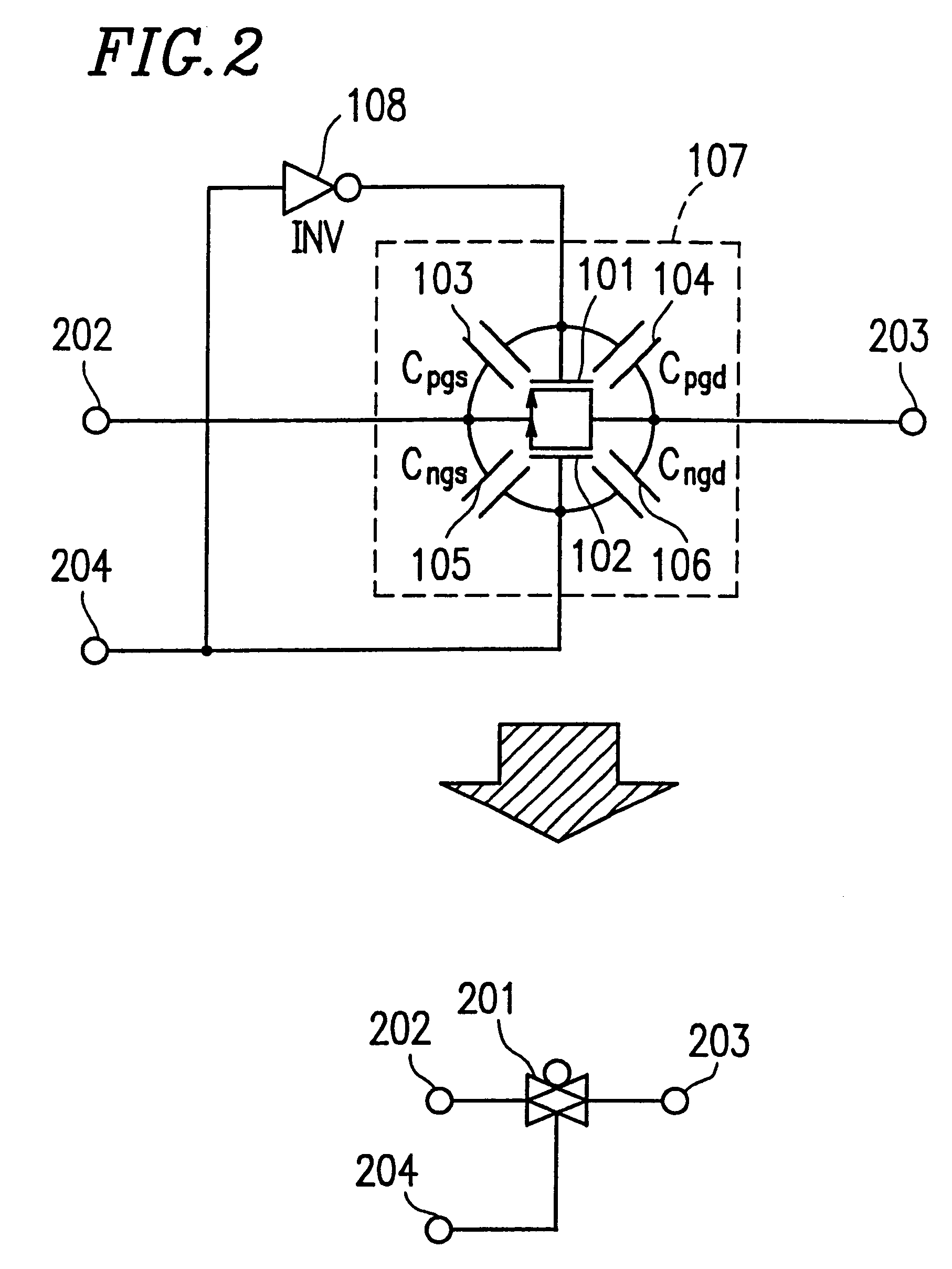
FIG. 2 shows a simplified representation of the CMOS type switch 107 and the inverter 108 illustrated in FIG. 1. The CMOS type switch 107 and the inverter 108 are a circuit which is equivalent to a switch 201 as illustrated in FIG. 2. In FIG. 2, reference numeral 202 denotes a switch input terminal, 203 a switch output terminal, and 204 a switch control terminal. A switch open / close control signal is applied to the switch control terminal 204.

The simplified representation as shown in FIG. 2 will be used in the following description.

FIG. 3 illustrates a configuration of an infrared radiation detection circuit 2 according to Embodiment 2 of the present invention, as an exemplary signal processing circuit for a charge generation type detection device.

The infrared radiation detection circuit 2 includes a charge-voltage conversion circuit 100a for converting a charge generated in the infrared sensor 109 to a voltage. In addition to the elements of the charge-voltage convers...

embodiment 3

While Embodiment 3 employs the single inverter 410, the present invention is not limited to this. The single inverter 410 may be replaced with a structure including an odd number (three or more) of such inverters serially connected together. Each of the odd number (three or more) of inverters is, for example, a CMOS type inverter.

(Embodiment 4)

FIG. 5 illustrates a configuration of an infrared radiation detection circuit 4 according to Embodiment 4 of the present invention, as an exemplary signal processing circuit for a charge generation type detection device.

The infrared radiation detection circuit 4 includes a charge-voltage conversion circuit 400a for converting a charge generated in the infrared sensor 109 to a voltage.

The charge-voltage conversion circuit 400a has a configuration where the FET 402 of the charge-voltage conversion circuit 400 illustrated in FIG. 4 is replaced with the switch 201.

As illustrated in FIG. 2, the switch 201 includes the CMOS type switch 107 having th...


PUM


Abstract

A signal processing circuit for a charge generation type detection device of the present invention includes a charge-voltage conversion circuit for converting a charge generated in the charge generation type detection device to a voltage. The charge-voltage conversion circuit includes: a first capacitor for storing the charge generated in the charge generation type detection device; an operational amplifier connected to the first capacitor to form a feed-back loop; and a first switch connected in parallel with the first capacitor for discharging the charge stored in the first capacitor. The first switch includes a first transistor for generating a first clock feed-through and a second transistor for generating a second clock feed-through, the first switch being configured so that at least a portion of the first clock feed-through is canceled by the second clock feed-through.

Description

BACKGROUND OF THE INVENTION1. Field of the InventionThe present invention relates to a signal processing circuit for use in a charge generation type detection device, such as a pyroelectric sensor, an infrared sensor, and a pressure sensor, including a charge-voltage conversion circuit for converting a charge generated in the charge generation type detection device to a voltage.2. Description of the Related ArtIn recent years, in the field of surveillance camera apparatuses, object sorting apparatuses, and the like, there has been a demand for a system capable of performing a high-level information processing operation by obtaining information such as the position, the size, and the traveling speed of an object, as well as the number of objects and whether the object is in contact with another object. For example, in order to realize high level security, a surveillance camera apparatus is required to detect infrared radiation from a human to produce such information.FIG. 8 illustrat...

Claims


Application Information

Patent Timeline
IPC IPC(8): G01L9/08
CPCG01L9/08
Inventor NAKATSUKA, JUNJI
Owner PANASONIC CORP
Why Eureka
Try Eureka