Non-volatile semiconductor memory device with reduced line resistance and method of manufacturing

a semiconductor memory and line resistance technology, applied in the direction of semiconductor devices, electrical devices, transistors, etc., can solve the problem of not being able to increase and achieve the effect of increasing the contact area and increasing the read-out speed of flash memory

Inactive Publication Date: 2002-08-20
NEC ELECTRONICS CORP
View PDF11 Cites 9 Cited by
  • Summary
  • Abstract
  • Description
  • Claims
  • Application Information

AI Technical Summary

Benefits of technology

By this arrangement, it is possible to increase the contact area between the metal wiring of a low resistivity and the control gate, whereb...

Problems solved by technology

Namely, the conventional structure has a drawback that it i...

Method used


Image

  • Non-volatile semiconductor memory device with reduced line resistance and method of manufacturing
  • Non-volatile semiconductor memory device with reduced line resistance and method of manufacturing
  • Non-volatile semiconductor memory device with reduced line resistance and method of manufacturing

Examples


Embodiment Construction

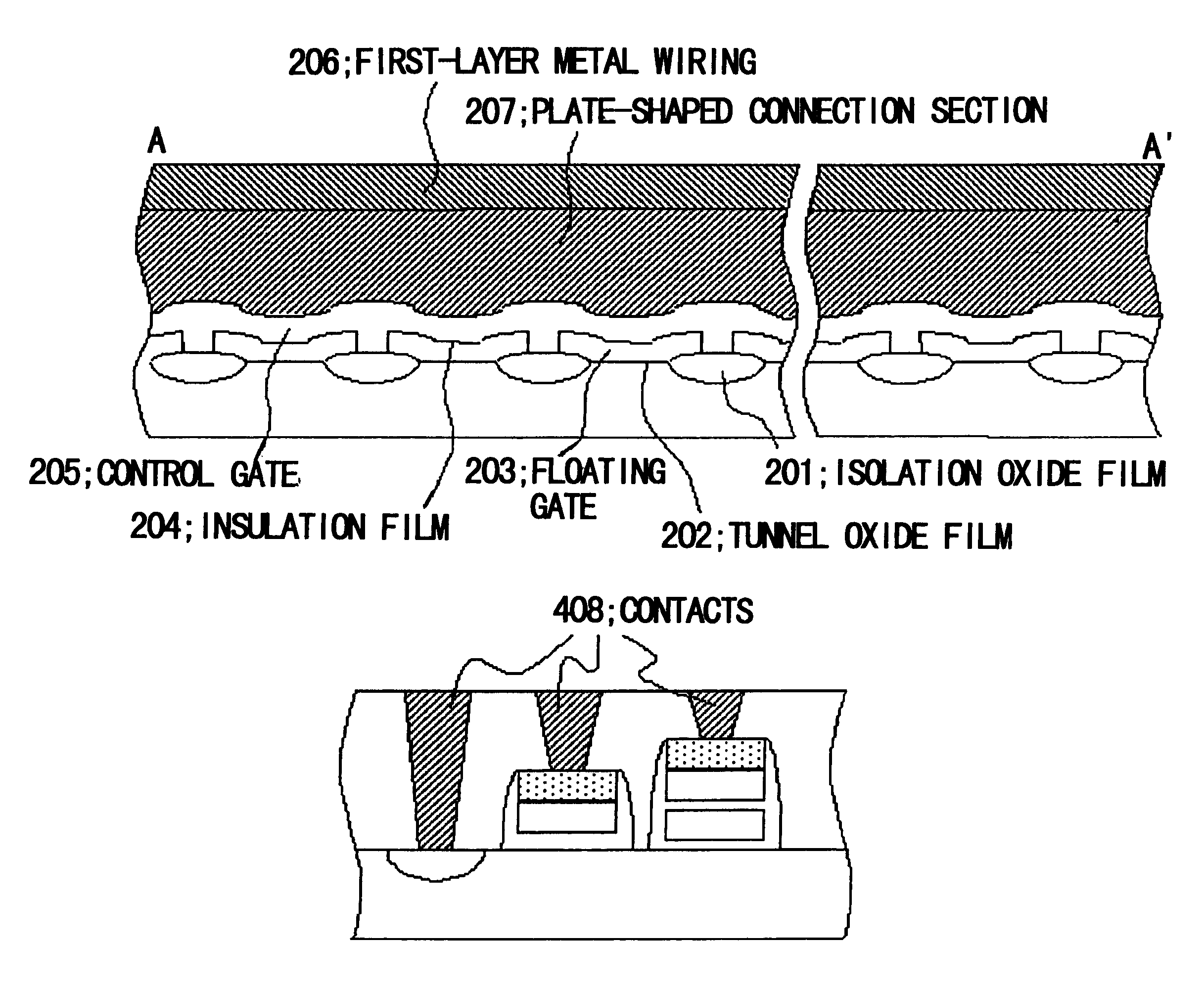
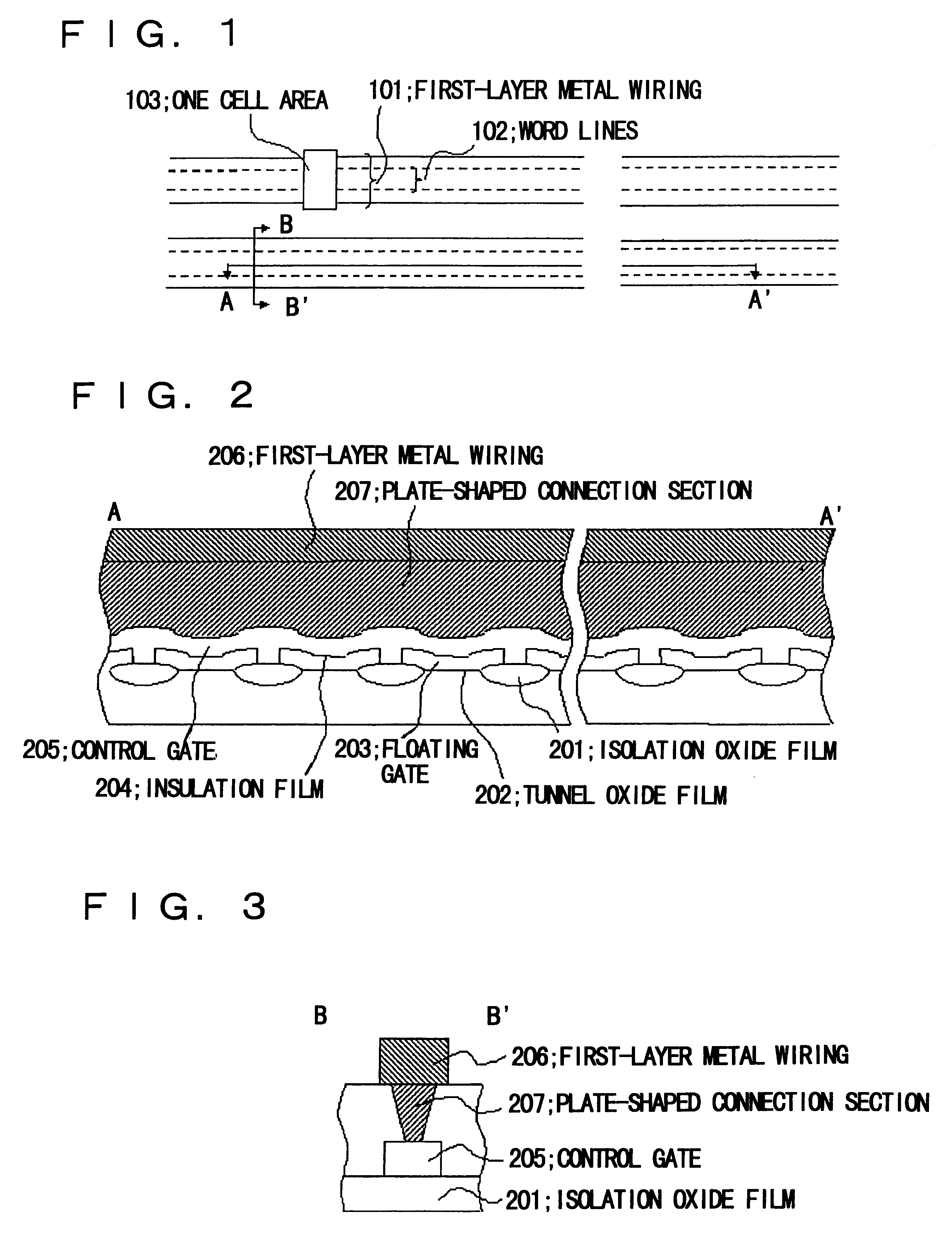
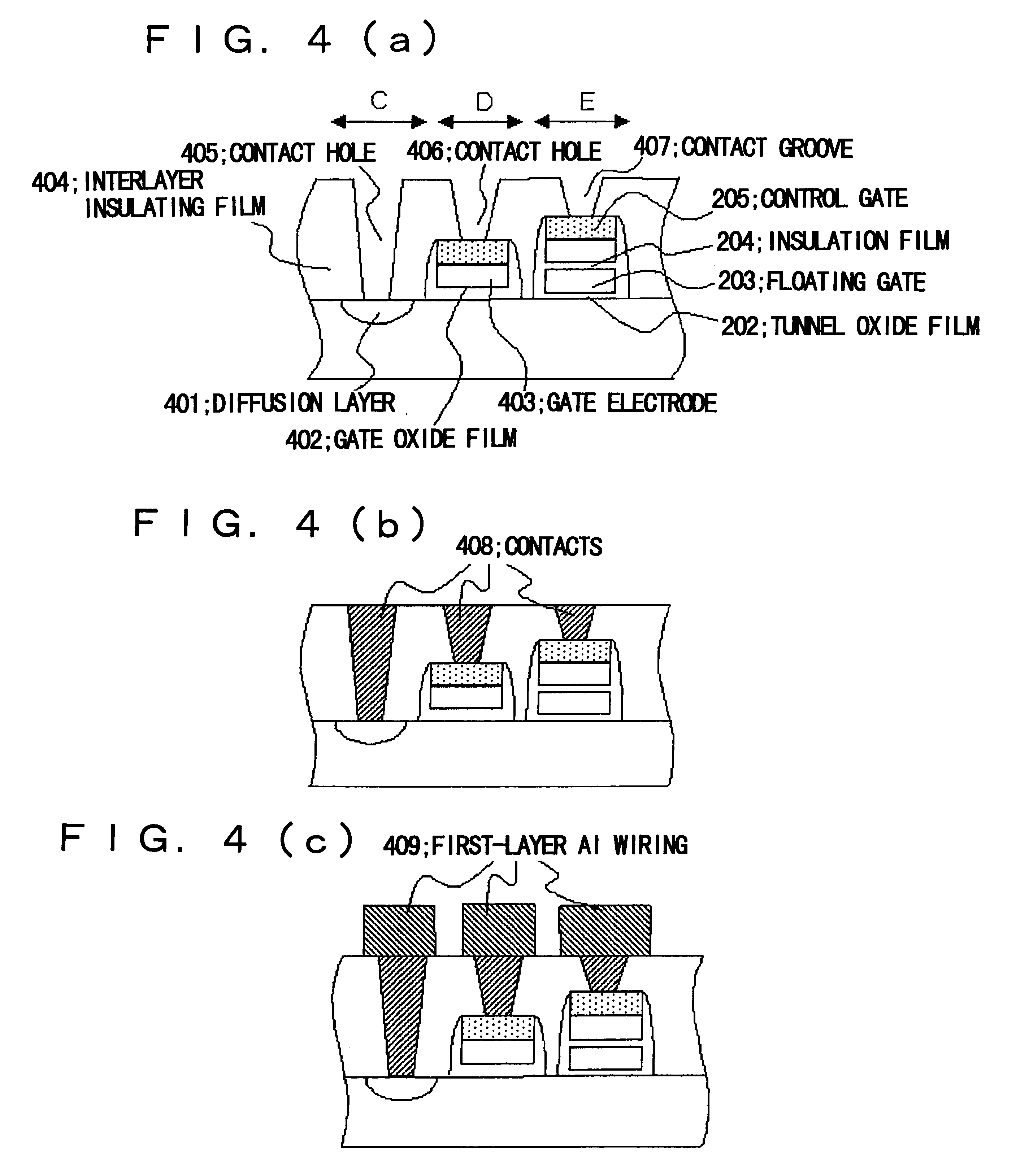
In a present embodiment according to the present invention, there is provided a non-volatile semiconductor memory device having a plurality of memory elements each having a floating gate (203 of FIG. 2) and a control gate (205 of FIG. 2), wherein there is formed, in an interlayer insulating film formed on the control gate, a contact groove (407 of FIG. 4(a)) passed through the interlayer insulating film (404 of FIG. 4a) and extending in the direction of a word line (102 of FIG. 1), and the contact groove is buried with an electrically conductive member of, for example, tungsten, whereby the metal wiring layer (409 of FIG. 4(c)) and the control gate are electrically connected with a large contact area.

By this arrangement, it is possible to increase the contact area between the metal wiring of a low resistivity and the control gate, whereby the wiring resistance between the word lines interconnecting the control gate can be reduced to increase the read-out speed of the flash memory.

DE...


PUM


Abstract

To provide a non-volatile semiconductor memory device in which the word line resistance can be decreased in resistance without being accompanied by increase in chip area, and a manufacturing method for the non-volatile semi conductor memory device. In a non-volatile semiconductor memory device having a floating gate (203 of FIG. 2) and a control gate (205 of FIG. 2), a contact groove (407 of FIG. 4a) extending in the direction of a word line (102 of FIG. 1) is provided on an interlayer insulating film (404 of FIG. 4a) formed as an upper layer of the control gate, and an electrically conductive member of, for example, tungsten, is embedded in the contact groove to establish electrical connection between the wiring metal (409 of FIG. 4d) formed as an upper layer of the interlayer insulating film and the control gate with a large contact area.

Description

This invent ion relates to a non-volatile semiconductor memory device and a manufacturing method thereof. More particularly, it relates to a non-volatile semiconductor memory device in which a word line is subjected to lining (or backing-up) a wiring as an overlaying layer to reduce the resistance, and a manufacturing method thereof.Up to now, lining of a word line of a flash memory has been practiced for reducing the resistance of the word line. However, since there was not much demand for high-speed accessing and the first layer wiring, used to be frequently allocated to a bit line, it was sufficient if a word line is connected to the second and following metal wiring layers substantially at a rate of one contact per 512 or 1024 cells so as to be used as lining. However, with the increase in the need for a flash memory embedded in a micro-computer and in the demand for high-speed accessing, it has come up to be felt necessary to raise the lining frequency. FIGS. 5 to 7 show an exa...

Claims


Application Information

Patent Timeline
IPC IPC(8): H01L27/105H01L21/8247H01L27/10H01L27/115H01L29/788H01L29/792
CPCH01L27/105
Inventor KAWATA, MASATOKIKUTA, KUNIKO
Owner NEC ELECTRONICS CORP
Why Eureka
Try Eureka