Radio frequency device with fast charging of an input capacitance

a radio frequency device and input capacitance technology, which is applied in gated amplifiers, amplifiers with semiconductor devices/discharge tubes, amplifiers, etc., can solve the problems of increasing switching time, and achieve the effect of minimizing the load effect of input transistors and high charging curren

Inactive Publication Date: 2002-08-20
CALLAHAN CELLULAR L L C
View PDF4 Cites 58 Cited by
  • Summary
  • Abstract
  • Description
  • Claims
  • Application Information

AI Technical Summary

Benefits of technology

to provide a highly linear gain-mode switchable radio frequency device that has a short switching on time when being switched from a low gain to a high gain mode.
It is another object of the invention to provide a single gain mode radio frequency device that has a short switching on time when being switched from off to on.
The invention is based on the insight that, by not relying on natural charging through biasing alone of the input transistor, when being switched from off to on, and / or from a low to a high gain mode, but by providing a charge boost to charge the input capacitance seen by the input transistor, the switching time can be greatly reduced.
In an advantageous embodiment of the invention, a high charging current is obtained through current amplification via a charging transistor. In order to minimize a load effect on the input transistor, the charging transistor is fully shut-off once charging of the capacitance is completed. Herewith, the charging process imposes minimal impact upon the input noise figure of the radio frequency device.

Problems solved by technology

The application of a large capacitance at the input electrode of the input transistor tends to increase the switching time because it takes too long for the large capacitor to charge it to the required turn on voltage, such a charging occurring `naturally` through the biasing.

Method used


Image

  • Radio frequency device with fast charging of an input capacitance
  • Radio frequency device with fast charging of an input capacitance
  • Radio frequency device with fast charging of an input capacitance

Examples


Embodiment Construction

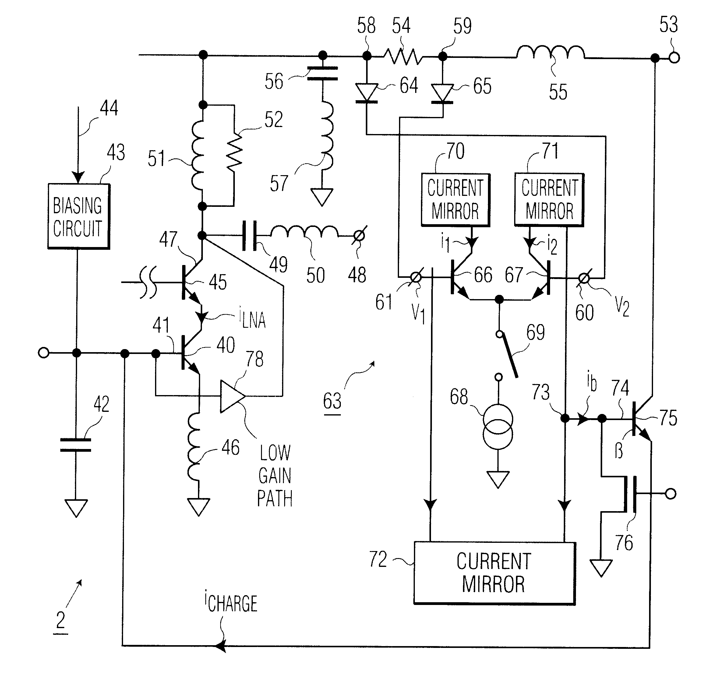
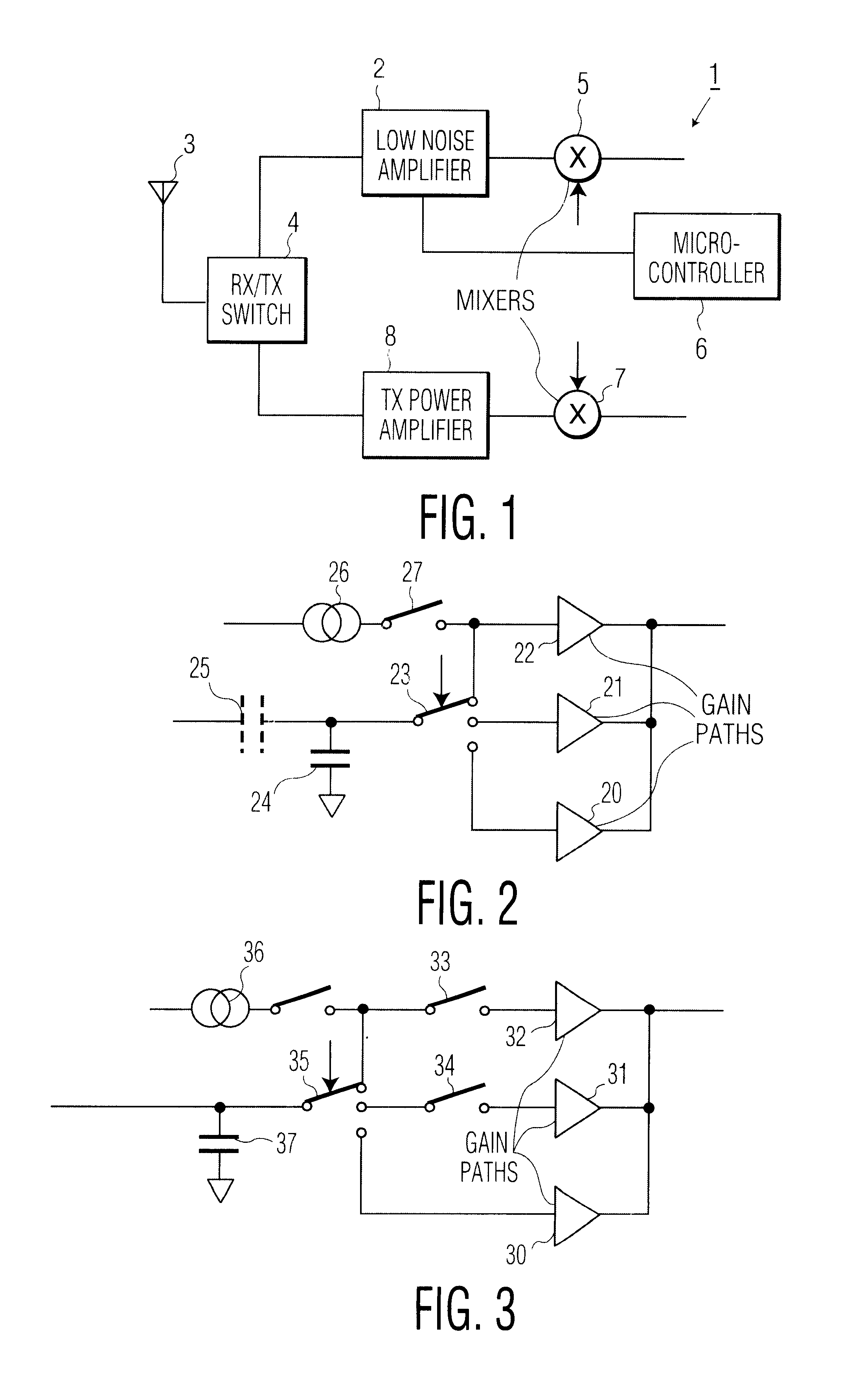
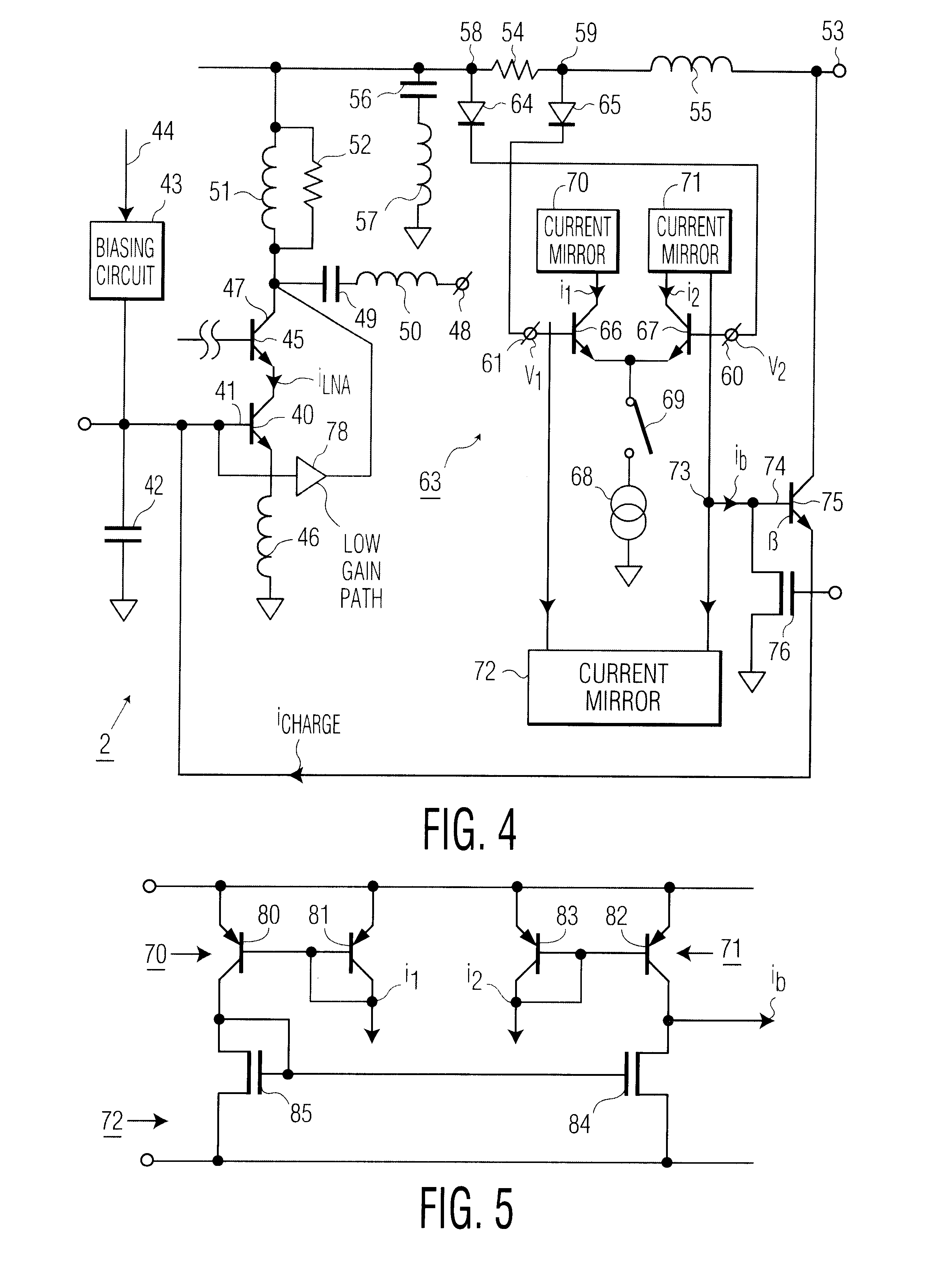
FIG. 1 is a block diagram of a transceiver 1 comprising a low noise amplifier 2 that is coupled, at input side, to an antenna 3 via a receive / transmit switch 4, and, at output side to a mixer of frequency down-converter 5. The transceiver further comprises a microcontroller 6 for controlling gain-mode switching and / or off to on switching of the low noise amplifier 2, a transmit mixer 7, and a transmit power amplifier 8. The invention is embodied in the low noise amplifier 2, but may be embodied in any other suitable radio frequency device, such as the mixer 5.

FIG. 2 schematically shows a gain path configuration of an embodiment of the low noise amplifier 2 as a radio frequency device according to the invention. The low noise amplifier 2 comprises three separate gain paths, a low gain path 20, a medium gain path 21, and a high gain path 22. The gain paths 20-22 are switchable by a controllable switch 23. At its input, the low noise amplifier 2 sees a capacitance, which may be a for r...


PUM


Abstract

A radio frequency device has an input transistor from which a capacitance is seen, and a fast charging circuit for charging the capacitance. The input transistor receives a radio frequency signal. The capacitance is quickly charged when the device is switched from off to on and / or from low gain to high gain, thereby reducing the switching-on time of the device.

Description

1. Field of the InventionThe present invention relates to a radio frequency device, more particularly to a radio frequency device that has an input transistor that sees a capacitance that needs to be charged when the radio frequency device is switched from off to on, and / or to a higher gain mode. Such a radio frequency device can be a low noise amplifier, a mixer, or any other suitable radio frequency device. The radio frequency device is used in a receiver, a transmitter, or transceiver, or the like.2. Description of the Related ArtGain-mode switchable devices such as low noise radio frequency amplifiers are known. Such devices have at least two switchable gain paths, a high gain path and a low gain path. Particularly in such systems as CDMA mobile radio systems, but also in many other systems, low noise radio frequency amplifiers should be highly linear. A key parameter to express linearity is the so-called Input Third Order Intercept Point (IIP3) of the amplifier. This is a measu...

Claims


Application Information

Patent Timeline
Patent Type & Authority Patents(United States)
IPC IPC(8): H03F1/08H03F3/72H03F1/30H03F1/32H03F1/22H04B1/40
CPCH03F1/22H03F1/305H03F1/32H03F3/72H03F2200/372H03F2200/391H03F2200/492H03F2203/45506H03F3/45085
Inventor WAITE, HELEN MARGARET
Owner CALLAHAN CELLULAR L L C
Why Eureka
Try Eureka