Method in the fabrication of a silicon bipolar transistor

a technology of bipolar transistors and fabrication methods, applied in the direction of basic electric elements, electrical apparatus, semiconductor devices, etc., can solve the problems of unlinking the intrinsic base, high base resistance, and requiring an additional mask layer

Inactive Publication Date: 2002-08-27
INFINEON TECH AG
View PDF21 Cites 36 Cited by
  • Summary
  • Abstract
  • Description
  • Claims
  • Application Information

AI Technical Summary

Benefits of technology

Extrinsic / intrinsic base structure for bipolar transistors is formed with low risk of affecting the existing base layer.Thick and highly doped polysilicon layers are created on extrinsic base regions.Amorphous silicon is utilized to improve doping profile and etching control of extrinsic base layer.No additional masks are used.In summary, the present invention provides a method of fabrication a semiconductor structure that utilizes a thin oxide as etch stop when opening the emitter window in a self-aligned silicon bipolar transistor.After formation of device isolation and deposition of intrinsic base, a thin oxide layer is deposited on the silicon used for intrinsic base before deposition of amorphous silicon for the extrinsic base. The structure is implanted by B or BF.sub.2 with dose parameter selected so that the entire dose is located within the amorphous silicon layer. Thin oxide will break up at subsequent heat treatments. After PETEOS deposition, the oxide / amorphous silicon is etched in emitter openings, using the thin oxide as an etch stop. Conventional processing finishes the device.It will be obvious that the invention may be varied in a plurality of ways. Such variations are not to be regarded as a departure from the scope of the invention. All such modifications as would be obvious to one skilled in the art are intended to be included within the scope of the appended claims.

Problems solved by technology

Several problems from the physics and practical point of view arise.
However, the method requires an additional mask layer, compared to conventional processing.
A common problem when fabricating self-aligned double-polysilicon bipolar transistors using thin bases is how to form the extrinsic base region (thick, heavily-doped material) and the intrinsic base region (thin, precise doping profile) and how to integrate this with the formation of the emitter.
The main problem occurs when the emitter window is to be opened.
The problem is how to stop the etching procedure so that the polycrystalline layer is fully removed without etching down into the substrate.
The problem is further accentuated if a thin base region formed via e.g. epitaxy prior to polysilicon deposition and etching of the emitter windows.
Especially when etching the emitter window, the etching properties is a major concern, since etching into the substrate (the intrinsic base), the base may be damaged or the link region between intrinsic and extrinsic base may be made too thin, causing high base resistance or even unlinking the intrinsic base from the extrinsic base.
Emitter pipes may also occur because of etching residues (pillars), which can cause emitter leakage currents.
Ion implantation into polycristalline materials is not an optimal choice if good doping profile control is required.
Because of channeling of the implanted species in polycristalline material, it may be hard to precisely control the doping profile.

Method used


Image

  • Method in the fabrication of a silicon bipolar transistor
  • Method in the fabrication of a silicon bipolar transistor
  • Method in the fabrication of a silicon bipolar transistor

Examples


Embodiment Construction

In the following description, for purposes of explanation and not limitation, specific details are set forth, such as particular techniques and applications in order to provide a thorough understanding of the present invention. However, it will be apparent to one skilled in the art that the present invention may be practiced in other embodiments that depart from these specific details. In other instances, detailed descriptions of well-known methods and apparatuses are omitted so as not to obscure the description of the present invention with unnecessary details.

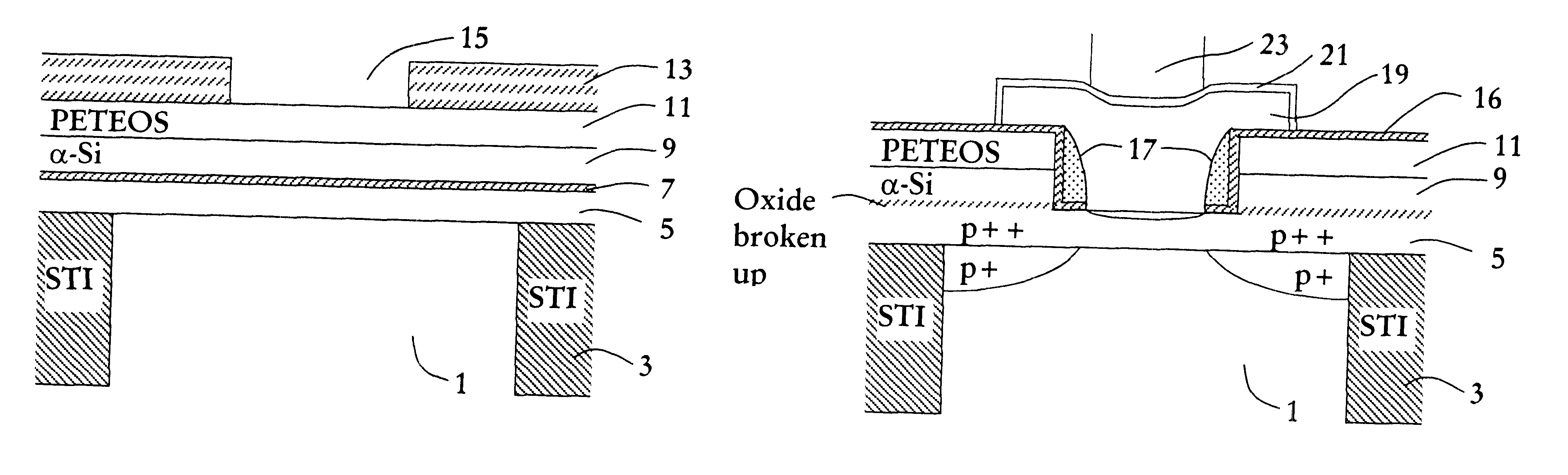
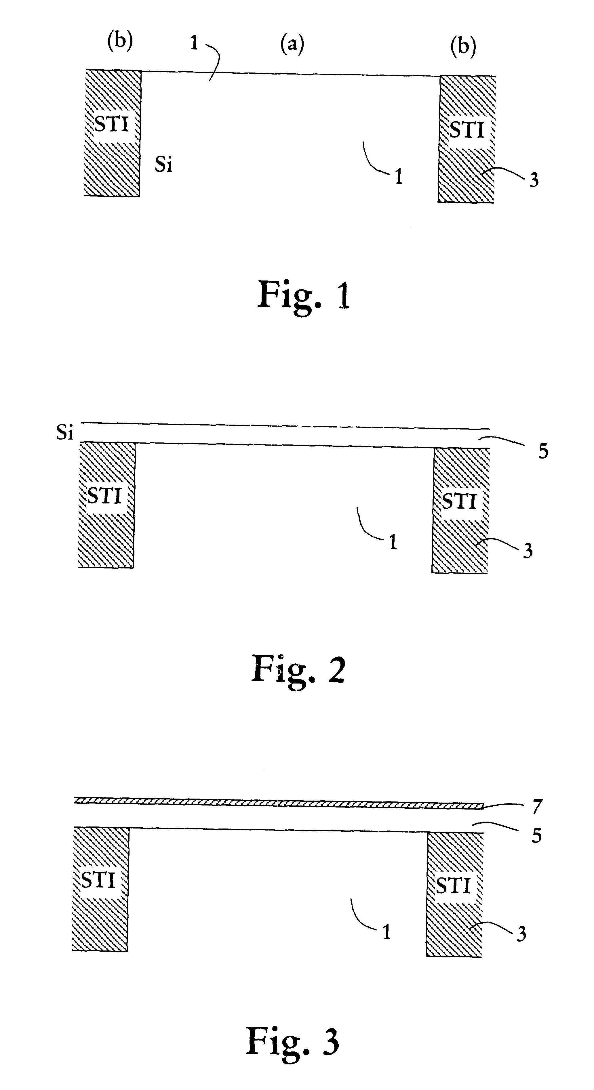
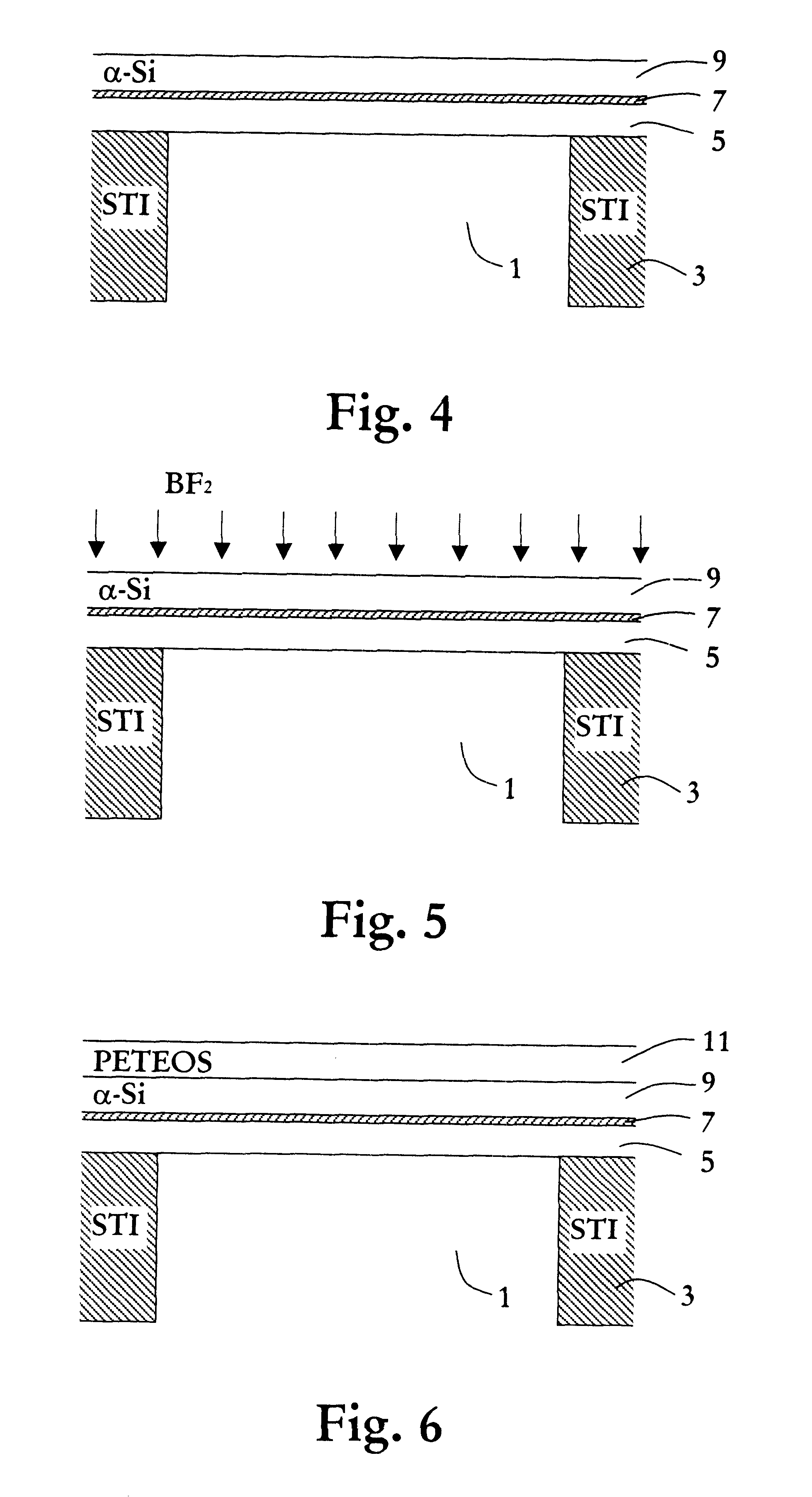
In this section, the process sequence, which includes formation of epitaxial base, extrinsic base and emitter window is described.

1. FIG. 1 shows a silicon substrate 1, which preferably is monocrystalline. The substrate can be homogeneous, but usually has different defined regions. In FIG. 1, the active area is depicted by (a), and isolation regions by (b). The substrate of the active area will form the collector of the devic...


PUM

PropertyMeasurementUnit
thicknessaaaaaaaaaa
thicknessaaaaaaaaaa
thicknessaaaaaaaaaa

Abstract

In the fabrication of a silicon bipolar transistor, a method for forming base regions and for opening an emitter window is provided. A silicon substrate is provided with suitable device isolation. A first base region is formed in or on top of the substrate. A thin layer of oxide is formed on the first base region. A layer of silicon is formed on top of the thin oxide layer, the silicon layer is to be a second base region. The silicon layer is ion implanted. A layer of a dielectric is formed on top of the silicon layer, the dielectric is to isolate base and emitter regions of the transistor. The obtained structure is patterned in order to define the emitter window. The structure inside the defined emitter window area is etched and through the dielectric and silicon layers, wherein the thin oxide layer is used as etch stop, thus forming the emitter window. The structure is subsequently heat treated and thus break up the oxide such that the first and second base regions will contact each other.

Description

The invention relates to silicon bipolar transistors, especially low-voltage high-frequency transistors for use in mobile telecommunications, and particularly it relates to a method in the fabrication of such transistors.TECHNICAL BACKGROUNDThe Problem AreaBipolar integrated circuits play a major role for modern telecommunication systems. The circuits are used mostly for analog functions, e.g. for switching currents and voltages, and for high-frequency radio functions (mixers, amplifiers, detector etc.).To achieve good high-frequency properties of the transistor, the base must be made very narrow. Several problems from the physics and practical point of view arise. The doping of the base must be carefully tuned to give a reasonable beta, not too high doping in the emitter-base junctions (low BV.sub.ebo will follow otherwise), enough doping to withstand voltage applied over the base without going into "punch-through" breakdown, the Early voltage should be high, base resistance should...

Claims


Application Information

Patent Timeline
Patent Type & Authority Patents(United States)
IPC IPC(8): H01L21/02H01L29/02H01L29/732H01L29/66H01L21/331H01L29/10H01L21/265
CPCH01L29/1004H01L29/66287H01L29/732
Inventor JOHANSSON, TEDNORSTROM, HANS
Owner INFINEON TECH AG
Why Eureka
Try Eureka