
Method of forming a pattern using proximity-effect-correction

a technology of proximity and pattern, applied in the field of pattern formation method using proximity effect correction, can solve problems such as pattern deformation

Inactive Publication Date: 2002-09-17
RENESAS ELECTRONICS CORP
View PDF16 Cites 38 Cited by
  • Summary
  • Abstract
  • Description
  • Claims
  • Application Information

AI Technical Summary

Problems solved by technology

In practice, however, there occurs pattern deformation such as that described above during production processes, and electrical characteristics of devices and various margins are influenced by the pattern deformation to a degree that cannot be neglected.

Method used


Image

  • Method of forming a pattern using proximity-effect-correction
  • Method of forming a pattern using proximity-effect-correction
  • Method of forming a pattern using proximity-effect-correction

Examples


first embodiment

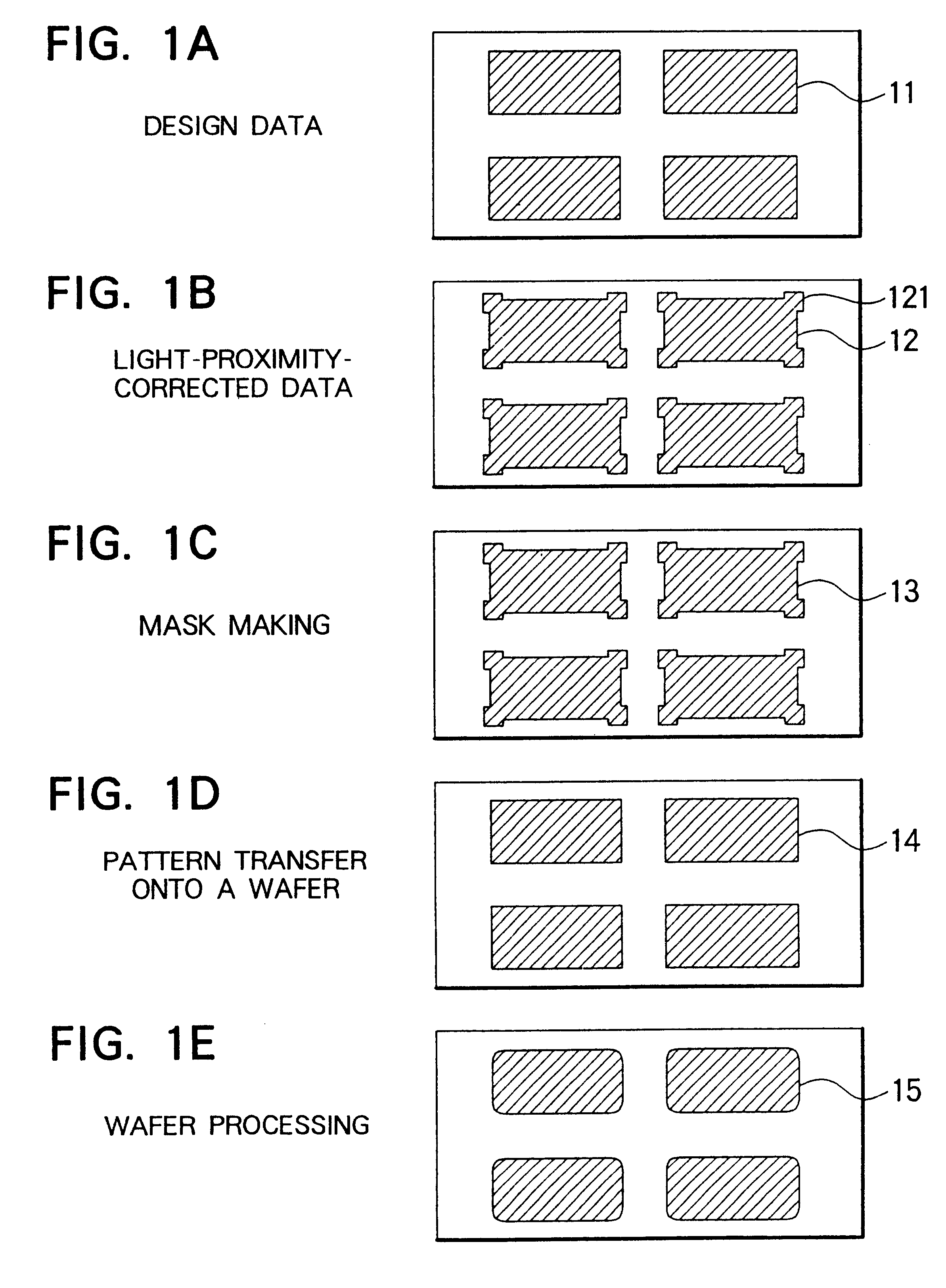
FIGS. 1A-1E are schematic diagrams illustrating a series of processing steps for forming a pattern according to the present invention. First, an LSI pattern such as that shown in FIG. 1A is designed using a CAD system or a similar tool so as to produce corresponding LSI pattern data consisting of a plurality of rectangular patterns 11. The designed data is then corrected according to the light proximity correction method which will be described in detail later so as to obtain light-proximity-corrected data as shown in FIG. 1B. The light-proximity-corrected data consists of a plurality of patterns 12 corresponding to the plurality of rectangular patterns 11 in the design data wherein each pattern 12 has auxiliary patterns 121 added at each corner so as to correct for pattern deformation due to diffraction of light which occurs during a process for transferring the pattern onto a wafer.

Electron beam exposure is then performed using the light-proximity-corrected data so that a mask inc...

embodiment 2

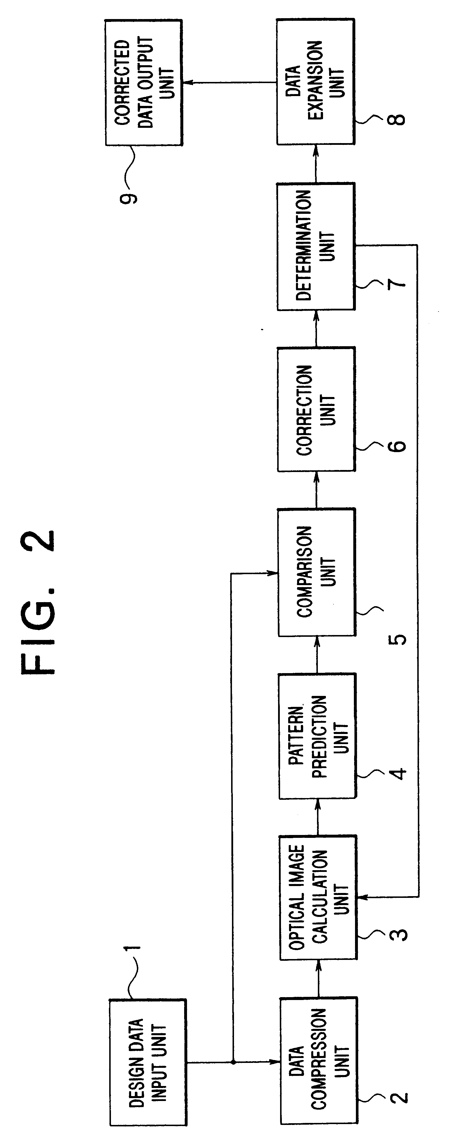
FIG. 2 is a block diagram illustrating a light proximity correction system used to accomplish the light proximity correction in the pattern formation process described in the first embodiment. Design data of an integrated circuit pattern produced with a CAD system is input to the system via a design data input unit 1. The design data input unit 1 is connected to a data compression unit 2 which performs data compression, in an pre-processing step, on the input data. The output of the data compression unit 2 is connected to an optical image calculation unit 3 for calculating an image which will be projected onto a wafer in a pattern transfer process. The output of the optical image calculation unit 3 is connected to a pattern prediction unit 4 for predicting the pattern which will be formed in-a resist as a result of the pattern transfer process. The pattern prediction unit 4 and the design data input unit 1 are connected to a comparison unit 5 for comparing the predicted pattern with...

embodiment 3

FIG. 4 is a block diagram of a light proximity correction system according to a third embodiment of the present invention. This system according to the third embodiment is the same as that according to the first embodiment shown in FIG. 2 except that the optical image calculation unit 3 is replaced by an optical image measurement unit 10 serving as the optical image formation unit defined in the first aspect of the invention. The optical image measurement unit 10 includes an optical system for measuring the image projected onto a wafer via a mask produced according to the design data. In the case of the second embodiment described above, the pattern image which will be projected onto a wafer is calculated in step S2 by means of software with the optical image calculation unit 3 from the compressed data. In the third embodiment, however, the projected image is measured by means of hardware with the optical image measurement unit 10 in step S9 after the data compression in step S1, as...


PUM


Abstract

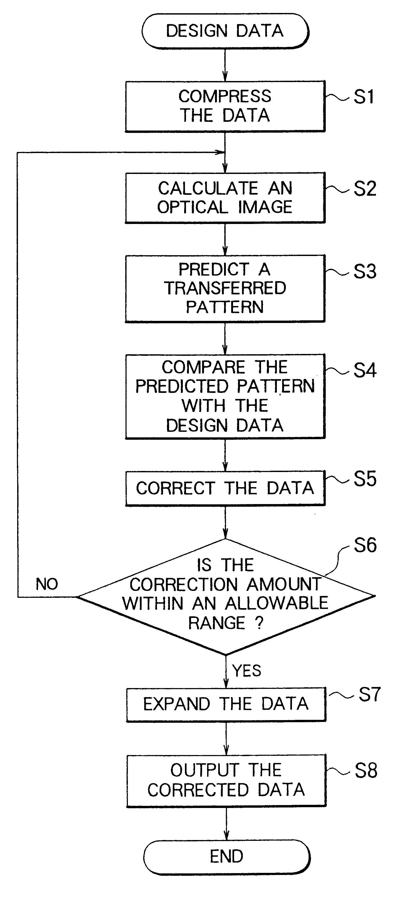
A method of correcting light proximity effects includes the steps of: compressing design data of a circuit pattern (step S1); generating a projection image which is formed during a process of transferring a pattern onto a wafer, the projection image being generated according to the design data (step S2); predicting the size of the transferred pattern, said prediction being performed from the projection image (step S3); calculating the difference between the predicted size of the transferred pattern and the pattern size designated by the design data (step S4); correcting the compressed design data by an amount equal to the above-described difference (step S5); judging whether the correction amount is within an allowable range (step S6); expanding the corrected data after the correction amount has fallen within the allowable range (step S7); and outputting the resultant data (step S8).

Description

1. Field of the InventionThe present invention relates to a system and method for correcting pattern data of an integrated circuit or the like so as to cancel the light proximity effects. The present invention also relates to a method of forming a pattern using such a method for correcting the light proximity effects.2. Description of the Related ArtReferring to FIGS. 29A to 29D, a conventional LSI production process will be described below. First, an LSI pattern such as that shown in FIG. 29A is designed using a CAD system or a similar tool and corresponding LSI pattern data is produced. The designed LSI pattern includes a plurality of rectangular patterns 291. Electron beam exposure is then performed according to the designed pattern data so as to produce a mask including a plurality of patterns 292 as shown in FIG. 29B. A wafer is exposed to ultraviolet light through the mask thereby transferring the pattern 292 formed on the mask onto the wafer. However, the pattern transferred ...

Claims


Application Information

Patent Timeline
IPC IPC(8): G03F7/20G06T9/00H01L21/82G03F1/36G03F1/68G03F1/70G06F17/50
CPCG03F7/70441G03F7/70616G06T9/004
Inventor KAMON, KAZUYA
Owner RENESAS ELECTRONICS CORP
Learn More