Emissive materials for organic light emitting devices
Inactive Publication Date: 2002-10-01
UNIV OF SOUTHERN CALIFORNIA +1
View PDF32 Cites 224 Cited by
Summary
Abstract
Description
Claims
Application Information
AI Technical Summary
This helps you quickly interpret patents by identifying the three key elements:
Problems solved by technology
Method used
Benefits of technology
Benefits of technology
Another advantage of the OLED devices of this invention is based on the use of both fluorescence and phosphorescence. The theoretical treatment of carrier recombination revealed that hole and electron recombination creates 25% of singlet exciton (which is fluorescence) and 75% of triplet exciton (which is phosphorescence). Thus, if we use fluorescent molecules as an emitter, we can use only 25% of fluorescence for EL and the EL efficiency is limited. However, when we use the molecules which possess both of fluorescence and phosphorescence characters, we could obtain 100% luminescence in principle. In ou
Problems solved by technology
For example, if the symmetry of an exciton is different from that of the ground state, then the radiative relaxation of the exciton is disallowed and luminescence will be slow and inefficient.
However, only a very few have been identified which are also capable of efficient room temperaturephosphorescence from triplets.
Thus, in most fluorescent dyes, the energy contained in the triplet states is wasted.
This typically restricts the Forster mechanism to transfers between singlet states.
Once excitons reach the guest triplet state, they are effectively lost since these fluorescent dyes typically exhibit extremely inefficient phosphorescence.
There are issues with the use of phosphorescence.
It has been noted that phosphorescent efficiency can decrease rapidly at high current densities.
It may be that long phosphorescent lifetimes cause saturation of emissive sites, and triplet-triplet annihilation may also produce efficiency losses.
Another issue is that triplet diffusion lengths are typically long (e.g., >1400 .ANG.) compared with typical singlet diffusion lengths of about 200 .ANG.. Thus, if phosphorescent devices are to achieve their potential, device structures need to be optimized for triplet properties.
Method used
Image
Click on the blue label to locate the original text in one second.
Reading with bidirectional positioning of images and text.
Examples
example 1
V.B.2. Example 1
The results for Example 1 were obtained using device 1, wherein device 1 has the following composition.
Device 1: ITO(120 nm) / TPD(50 nm) / Zn(BOX).sub.2 (specifically the molecule of formula 1, below)2.8%-CBP(20 nm) / BCP(10 nm) / Alq3(20 nm) / MgAg(150 nm) / Ag(50 nm) wherein
ITO is a transparent conducting phase of indiumtinoxide which functions as an anode.
ITO is a degenerate semiconductor formed by doping a wide bandsemiconductor. The carrier concentration of the ITO is in excess of 10.sup.19 / cm.sup.3. The number 120 nm (=1200 .ANG.) is the thickness of the ITO layer.
and MgAg(thickness 150 nm) / Ag(thickness50 nm) as a cathodeelectrode.
The chemical names are used as in Example 1.
The results for Example 2 / device 2 are given in FIGS. 5 through 8.
V. C. Other Molecular Depictions
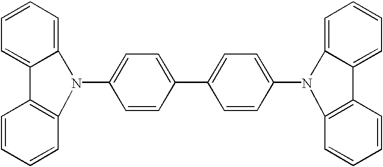
A molecule for the hole-transporting layer of the invention is depicted below. ##STR24##
The invention will work with other hole-transporting molecules known by one of ordinary skill to work in hole transporting layers of OLEDs.
The molecule which u...
PUM
Property
Measurement
Unit
Efficiency
aaaaa
aaaaa
Fluorescence
aaaaa
aaaaa
Phosphorescence quantum yield
aaaaa
aaaaa
Abstract
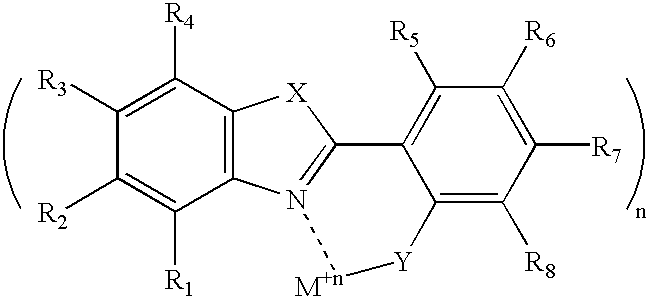
Improved electroluminescent efficiency in organic light emitting diodes is obtained with an emitter layer comprising organic complexes of transition metals with benzoxazole derivatives. A dimethylated benzoxazole derivative with zinc shows blue fluorescence and phosphorescence.
Description
I. FIELD OF INVENTIONThe present invention is directed to the use of organometallic compounds, especially of certain benzoxazoles with transition metals, as dopants in certain hosts as emitters in organic light emitting diodes.II. BACKGROUND OF THE INVENTIONII. A. General BackgroundOrganic light emitting devices (OLEDs) are comprised of several organic layers in which one of the layers is comprised of an organic material that can be made to electroluminesce by applying a voltage across the device, C. W. Tang et al., Appl. Phys. Lett. 1987, 51, 913. Certain OLEDs have been shown to have sufficient brightness, range of color and operating lifetimes for use as a practical alternative technology to LCD-based full color flat-panel displays (S. R. Forrest, P. E. Burrows and M. E. Thompson, Laser Focus World, Feb. 1995). Since many of the thin organic films used in such devices are transparent in the visible spectral region, they allow for the realization of a completely new type of displa...
Claims
Application Information
Patent Timeline
Application Date:The date an application was filed.
Publication Date:The date a patent or application was officially published.
First Publication Date:The earliest publication date of a patent with the same application number.
Issue Date:Publication date of the patent grant document.
PCT Entry Date:The Entry date of PCT National Phase.
Estimated Expiry Date:The statutory expiry date of a patent right according to the Patent Law, and it is the longest term of protection that the patent right can achieve without the termination of the patent right due to other reasons(Term extension factor has been taken into account ).
Invalid Date:Actual expiry date is based on effective date or publication date of legal transaction data of invalid patent.

