Anode assembly for plating and planarizing a conductive layer

Inactive Publication Date: 2002-11-12
NOVELLUS SYSTEMS
View PDF48 Cites 50 Cited by
  • Summary
  • Abstract
  • Description
  • Claims
  • Application Information

AI Technical Summary

Benefits of technology

Another feature of the invention is that the anode assembly additionally includes a spindle to which the shaft is mounted and by which rotati

Problems solved by technology

In practice, it is difficult to obtain a metal layer with

Method used


Image

  • Anode assembly for plating and planarizing a conductive layer
  • Anode assembly for plating and planarizing a conductive layer
  • Anode assembly for plating and planarizing a conductive layer

Examples


Embodiment Construction

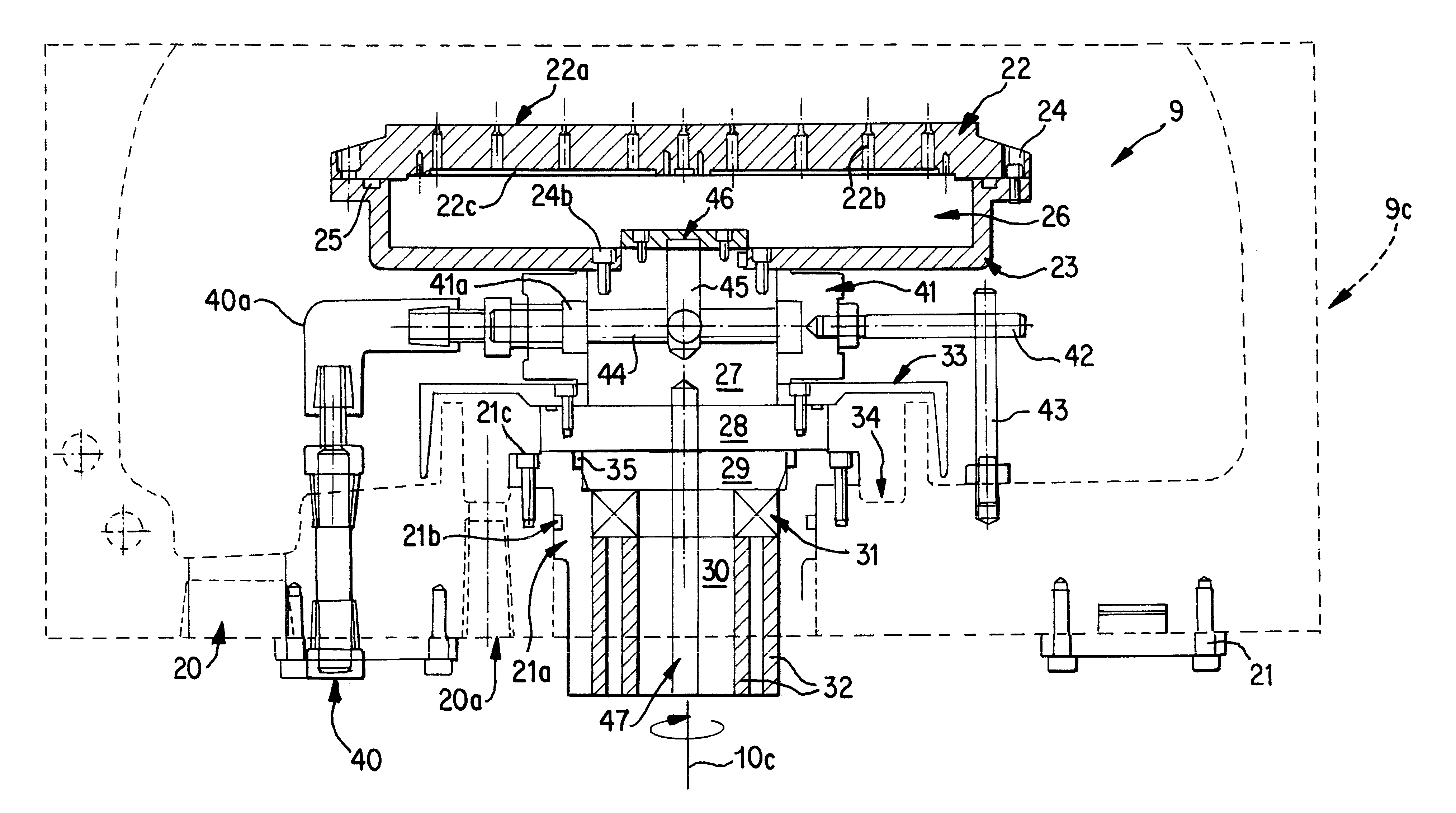
A general depiction of a plating and planarization apparatus in which the anode assembly of this invention can be used is shown in FIG. 2. The carrier head 10 holds a round semiconductor wafer 16 and, at the same time, provides an electrical lead 7 connected to the conductive lower surface of the wafer. The head can be rotated about a first axis 10b. The head can also be moved in the x and z directions represented in FIG. 2. An arrangement which provides movement in the y direction may also be provided for the head.

Certain embodiments of a carrier head that may be used to hold the wafer 16 form the subject matter of co-pending U.S. patent application Ser. No. 09 / 472,523, titled WORK PIECE CARRIER HEAD FOR PLATING AND POLISHING, filed Dec. 27, 1999.

A pad 8 is provided on top of a round anode assembly 9 across from the wafer surface. The pad 8 may have designs or structures such as those forming the subject matter of co-pending U.S. patent application Ser. No. 09 / 511,278, titled PAD D...


PUM

PropertyMeasurementUnit
Electric potential / voltageaaaaaaaaaa

Abstract

A particular anode assembly can be used to supply a solution for any of a plating operation, a planarization operation, and a plating and planarization operation to be performed on a semiconductor wafer. The anode assembly includes a rotatable shaft disposed within a chamber in which the operation is performed, an anode housing connected to the shaft, and a porous pad support plate attached to the anode housing. The support plate has a top surface adapted to support a pad which is to face the wafer, and, together with the anode housing, defines an anode cavity. A consumable anode may be provided in the anode cavity to provide plating material to the solution. A solution delivery structure by which the solution can be delivered to said anode cavity is also provided. The solution delivery structure may be contained within the chamber in which the operation is performed. A shield can also be mounted between the shaft and an associated spindle to prevent leakage of the solution from the chamber.

Description

BACKGROUND OF THE INVENTIONMulti-level integrated circuit manufacturing requires many steps of metal and insulator film depositions followed by photoresist patterning and etching or other means of material removal. After photolithography and etching, the resulting wafer or substrate surface is non-planar and contains many features such as vias, lines or channels. Often, these features need to be filled with a specific material, such as a metal, a dielectric, or both. For high performance applications, the wafer topographic surface needs to be planarized, making it ready again for the next level of processing, which commonly involves deposition of a material, and a photolithographic step. It is most preferred that the substrate surface be flat before the photolithographic step so that proper focusing and level-to-level registration or alignment can be achieved. Therefore, after each deposition step that yields a non-planar surface on the wafer, there is often a step of surface planar...

Claims


Application Information

Patent Timeline
IPC IPC(8): C25F7/00C25D17/10C25D17/14C25D7/12C25D17/12C25F3/30H01L21/288H01L21/306
CPCC25D17/14C25F7/00C25D17/00
Inventor VOLODARSKY, RIMMAVOLODARSKY, KONSTANTINUZOH, CYPRIANTALIEH, HOMAYOUNYOUNG, DOUGLAS W.
Owner NOVELLUS SYSTEMS
Why Eureka
Try Eureka