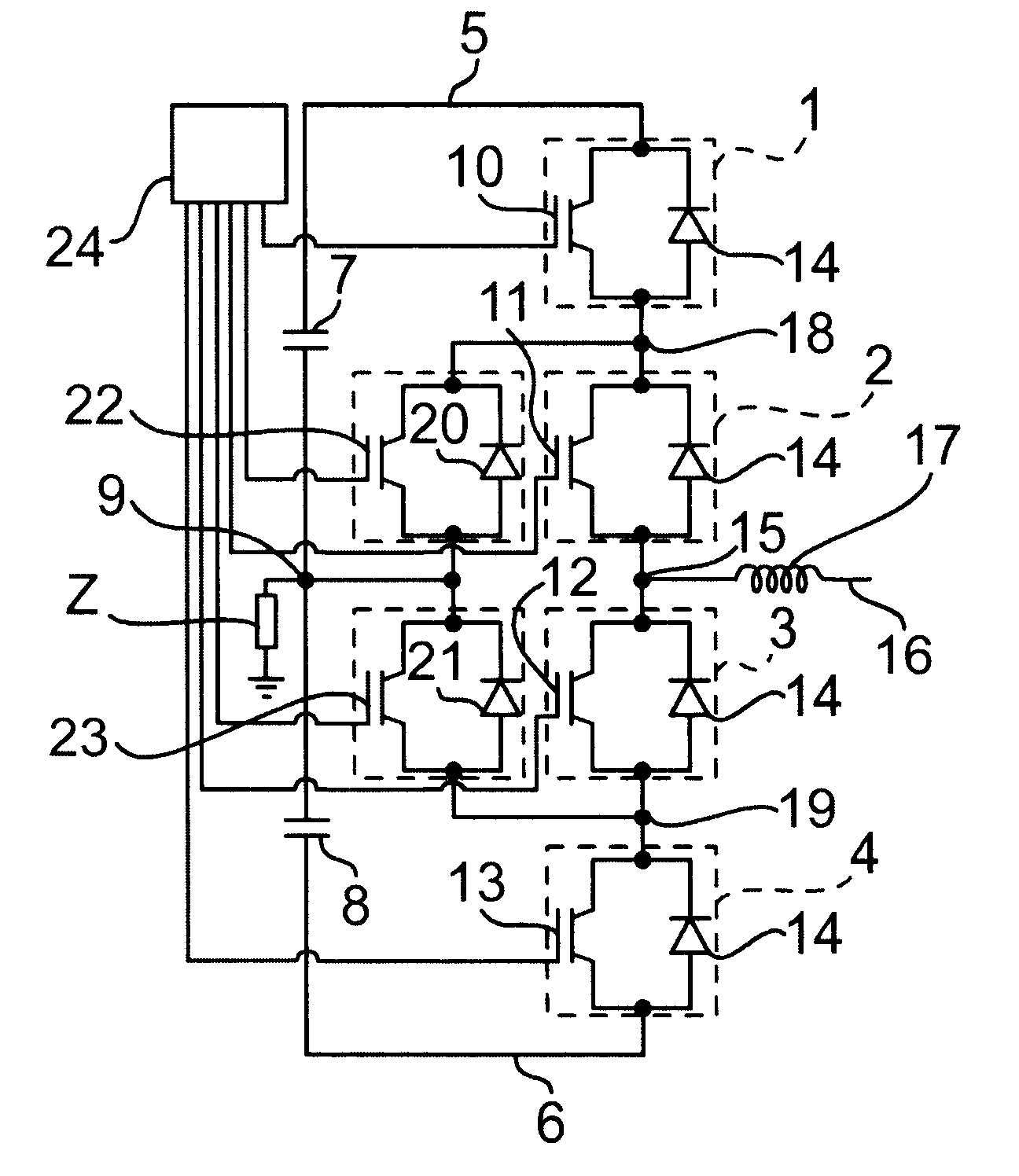
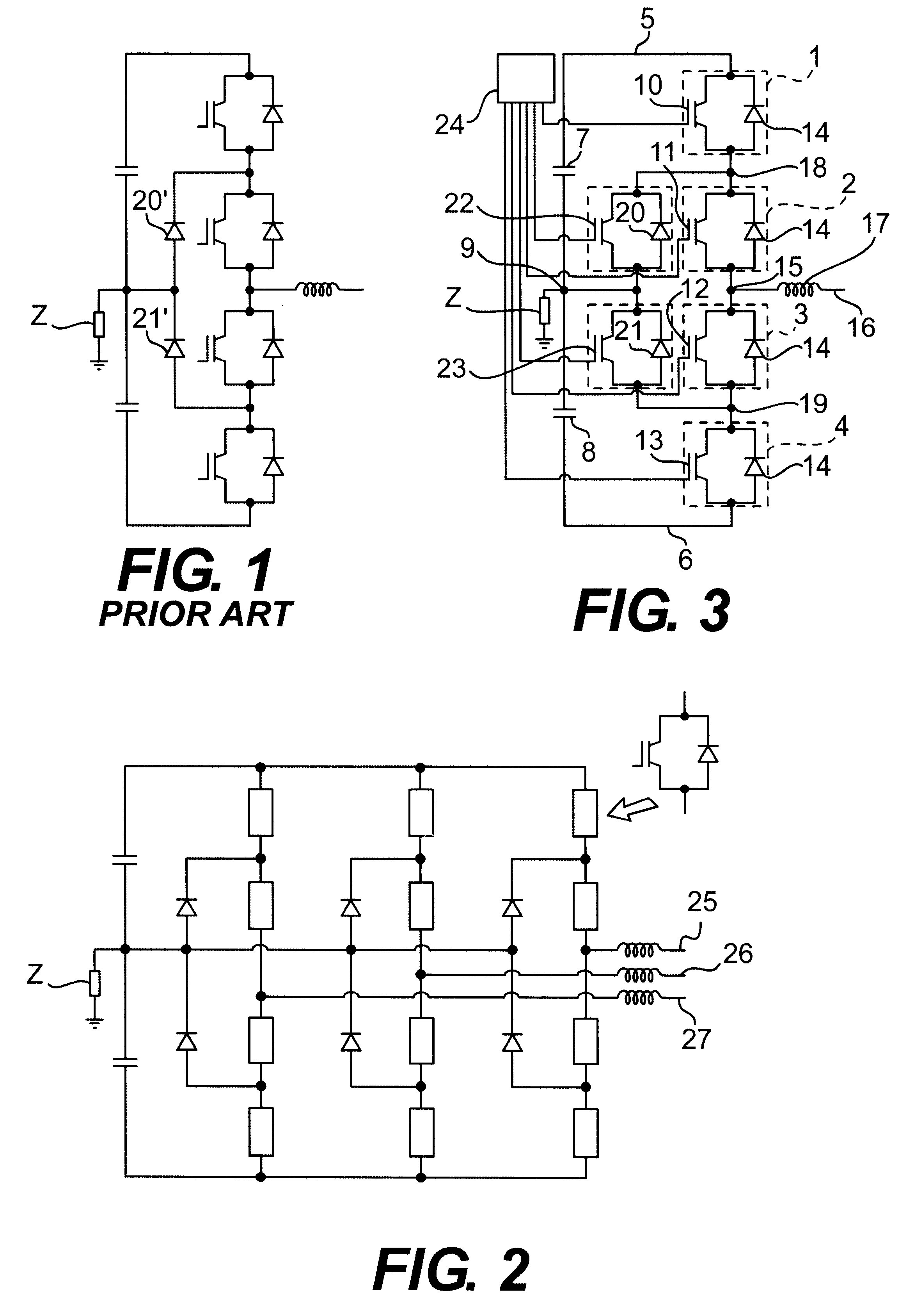
By arranging a semiconductor element of turn-off type in this way in anti-parallel with said second diodes it is possible to also control the connection of the mid point of the direct voltage side to the second mid point, and it gets possible to obtain a desired
pulse width modulation pattern at the connection of the phase line to the phase output by turning these semiconductor elements on and off as well as those arranged between said second mid point and the respective pole with a comparatively
low frequency in the order of the
fundamental frequency of the alternating voltage of the alternating voltage phase line, whereas the semiconductor elements of the "inner" units are turned on and off with a significantly higher frequency, more exactly the so called real
pulse width modulation frequency. The frequency through which the semiconductor elements first mentioned are switched may for example be 50 or 60 Hz, while the pulse width modulation frequency is typically 1-2 kHz. This means that totally different, more exactly lower, demands are made upon the semiconductor elements first mentioned, which have not to be turned on and turned off with any
high frequency, which means that for this semiconductor elements having a considerable better ability to hold high voltages may be used, since such
high voltage semiconductor elements cannot take high frequencies without unacceptably high switching losses. Voltages in the order of 10-400 kV are normally handled in devices of this type, and this requires then a series connection of a higher number of semiconductor elements within each said unit for a series connection of a higher number of said units so as to distribute the voltage these have to hold in the blocking state among a high number of such semiconductor elements. Thus, in the present case it will be possible to use a lower number of semiconductor elements connected in series between said second mid point and the respective pole, since these may be of
high voltage type, for example hold 4-6 kV instead of 2-3 kV, which means a considerable saving of costs and simplifies the control of the device.
Semiconductor elements with a smaller component area may alternatively be used, which have a higher
thermal resistance, but which are available to a low cost, may be used for these semiconductor elements switched comparatively seldom. The same condition is valid for the semiconductor elements connected in anti-parallel with the second diodes and switched with a low
switching frequency.
According to a preferred embodiment of the invention the apparatus is adapted to control the semiconductor elements connected in anti-parallel with said second diodes and in the units between the respective second mid point and the respective pole with a frequency coinciding with said fundamental frequency in absence of voltage
harmonics in the alternating voltage phase line. A large difference in frequency between the control of these semiconductor elements and the other semiconductor elements is obtained by this and the advantages mentioned above of the invention with respect to the devices already known will by this be very remarkable. The apparatus is advantageously adapted, when said voltage
harmonics occur to optionally carry out one or several additional switchings of the semiconductor elements connected in anti-parallel with said second diodes and those in the units between the respective second mid point and the respective pole within a fundamental frequency period, in which a switching is defined as comprising a turn-off and turn-on. It may in this way be compensated for such instabilities, in which the frequency in question may during a very short period of time become for example three times said fundamental frequency, but it is still considerably lower than the pulse width modulation frequency.
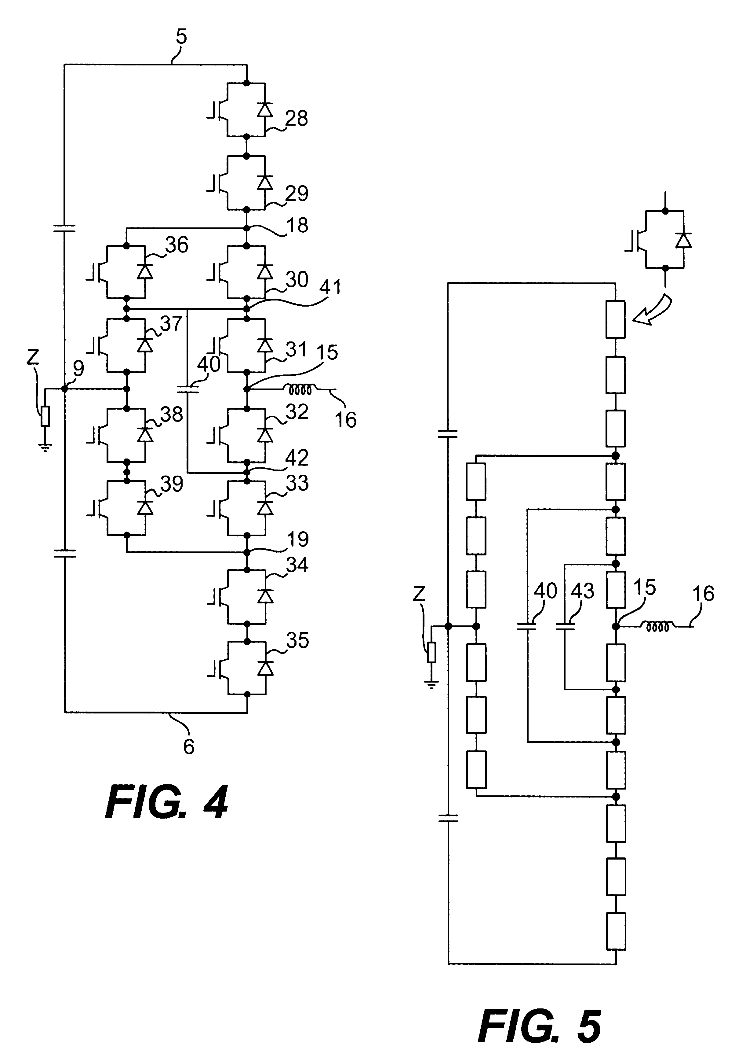
According to a preferred embodiment of the invention n is 5 and said units are adapted to give the
flying capacitor a voltage across the poles thereof substantially equal to U / 4n, in which U is the voltage between the two poles of the direct voltage side. The voltage of the
flying capacitor may in this way be kept low and the size and the cost thereof may be kept at a low level.
According to another preferred embodiment of the invention the apparatus is adapted to control said units, when one pole of said flying capacitors is connected to said phase output so that the phase current passes said
capacitor, to make this connection in one of two ways, which gives substantially the same phase potential on the phase outlet depending upon the instantaneous real level of the voltage between the poles of the
capacitor, so that the
capacitor is upon said connection charged for a voltage level thereof lower than desired and discharged for a voltage level thereof higher than desired. This process is possible thanks to the fact that there are two possible states giving almost the same potential on the phase output, in which one state may be used for charging the capacitor and the other for discharging the capacitor for a given direction of the phase current. This process means that the
capacitance value of the capacitor may be kept at a minimum, with a
time constant for the charging and the discharging, respectively, which is a suitable factor higher than the period of time during which the capacitor is normally switched in each of the positions for a given
switching frequency.


