Multi-cavity substrate structure for discrete devices

a substrate structure and discrete device technology, applied in the direction of semiconductor/solid-state device details, printed circuit non-printed electric components association, printed circuit aspects, etc., can solve the problems of voltage surge, ground plane bounce, stray inductance, etc., to reduce the length of signal leads

Inactive Publication Date: 2002-12-03
IBM CORP
View PDF8 Cites 59 Cited by
  • Summary
  • Abstract
  • Description
  • Claims
  • Application Information

AI Technical Summary

Benefits of technology

is to provide a method and structure to minimize the l...

Problems solved by technology

As the distance from the capacitor to the semiconductor device increases, the capacitor's efficiency and effectiveness are adversely affected.
Problems that can occur include stray inductances, ground plane bounce...

Method used


Image

  • Multi-cavity substrate structure for discrete devices
  • Multi-cavity substrate structure for discrete devices
  • Multi-cavity substrate structure for discrete devices

Examples


Embodiment Construction

)

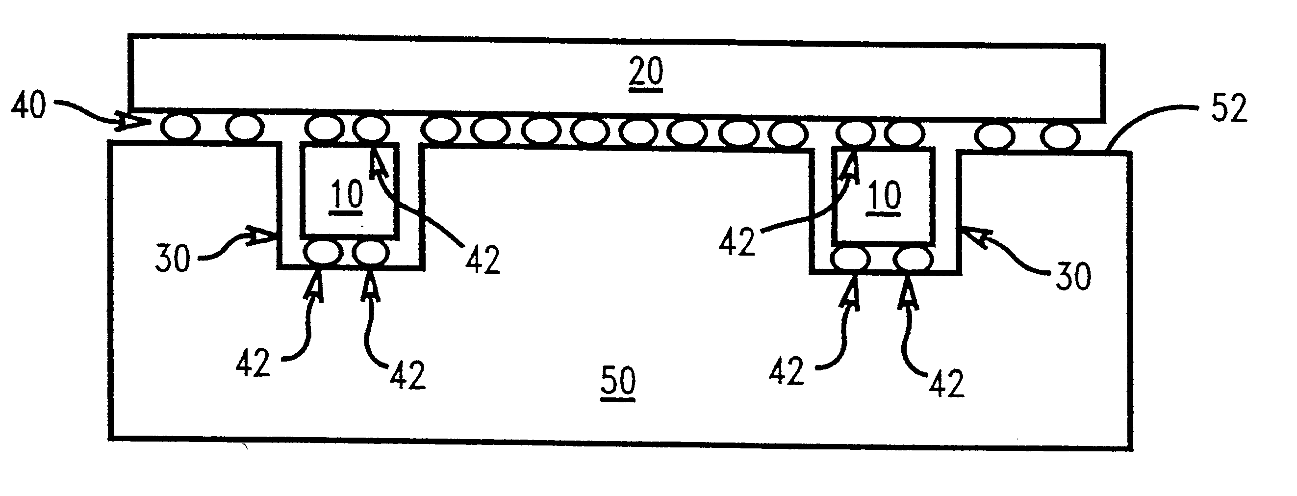
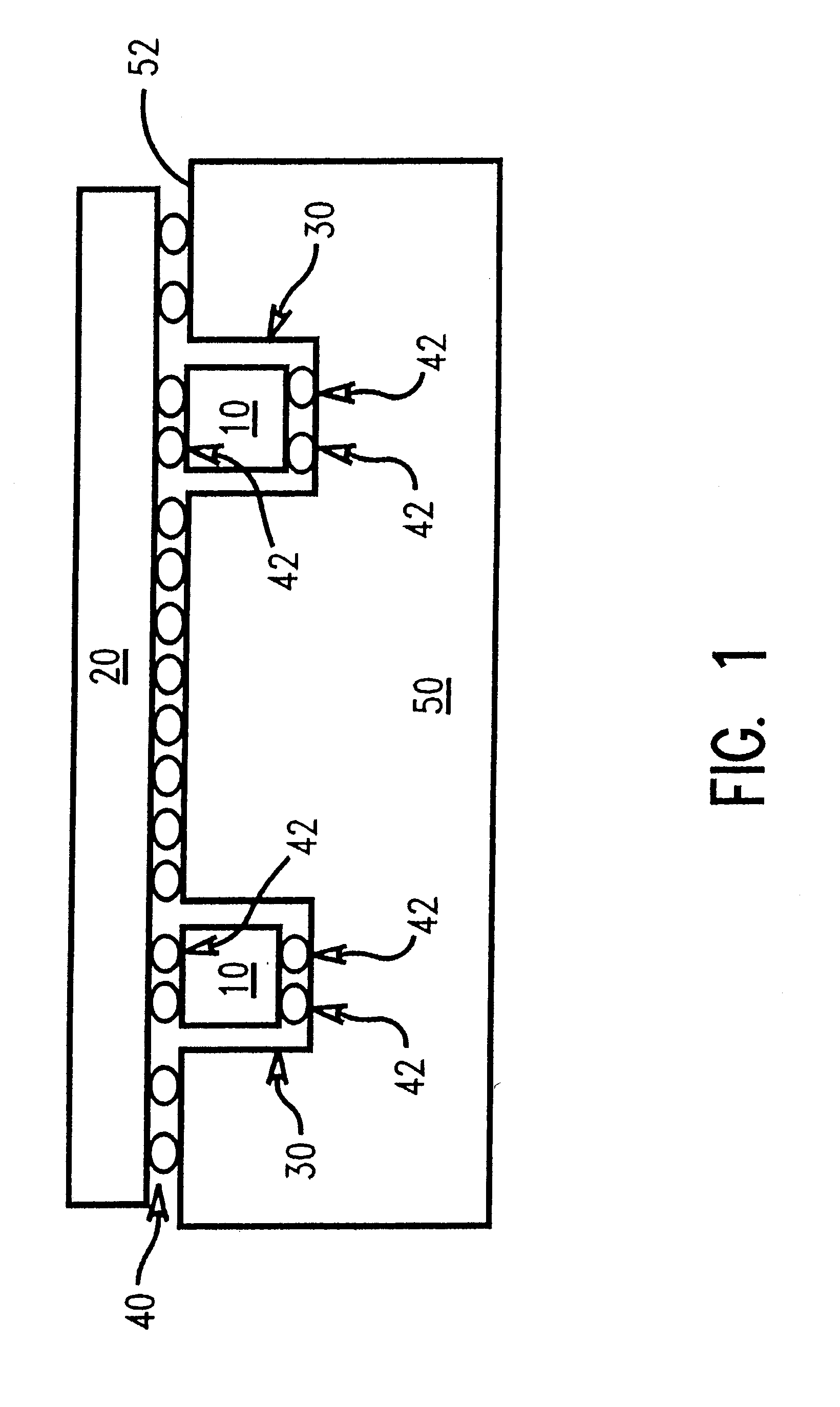
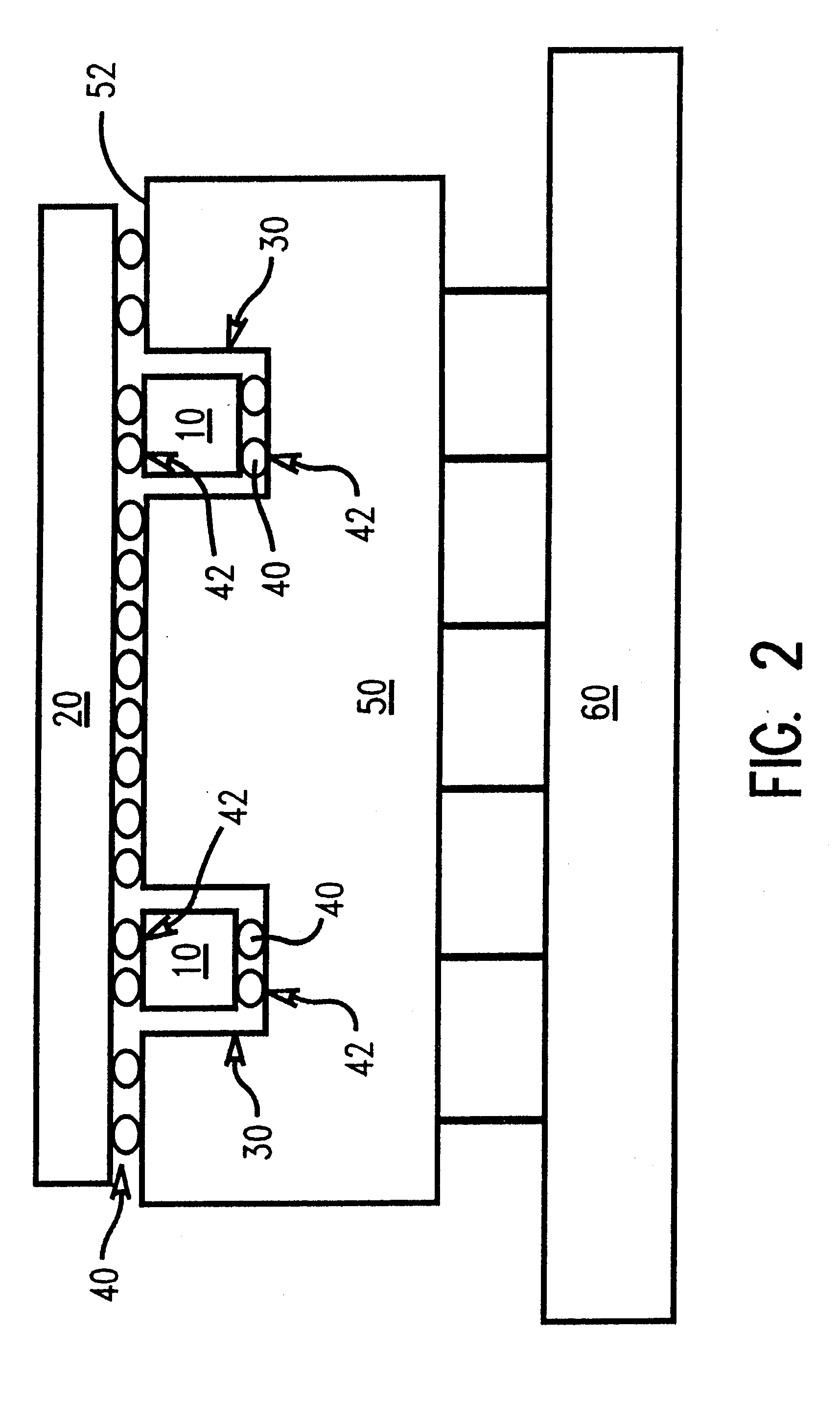
In describing the preferred embodiment of the present invention, reference will be made herein to FIGS. 1-4 of the drawings in which like numerals refer to like features of the invention. Features of the invention are not necessarily shown to scale in the drawings.

In the present invention, one or more passive electronic components 10 are mounted within the body of a carrier or board 50 by creating a cavity 30 in a substrate or carrier 50 that is directly below a semiconductor device 20 and electrically contacting substrate 50 and device 20 to component 10, as shown in FIG. 1. This results in a much shorter lead length for the passive component 10. A typical carrier 50 includes a plurality of layers including internal wiring including vias, power planes and transmission lines. Carrier 50 may comprise ceramic, glass, organic, silicon materials or any commonly known semiconductor device carrier structure. Carrier 50 with passive components 10 and device 20 may be attached to an integr...


PUM


Abstract

The distance between a discrete or passive electrical component and an electrical semiconductor device and substrate or carrier is minimized by shortening the lead length connections of the passive component. One or more passive electronic components are mounted within the body of a carrier or board by creating a cavity in the substrate or carrier that is directly below a semiconductor device. The passive component is electrically connected to the substrate and device using solder bump technology resulting in much shorter lead length connections to and from the passive component.

Description

1. Field of the InventionThe present invention relates generally to integrated circuit packaging, and in particular to a structure and method for minimizing the lead length between a passive electronic device and an integrated circuit.2. Description of Related ArtSemiconductor devices having high and dense lead counts and operating at high speeds require very short leads to ensure noiseless signal propagation. Noise can be introduced onto a lead by other nearby signal leads. Additionally, passive devices or components, such as resistors, capacitors, inductors and filters, add to the length of signal leads within an assembly. As used herein, the term "semiconductor device" or "device" refers to an integrated circuit chip or die containing circuitry. The "carrier" refers to the substrate material upon which the device is attached and contains internal circuitry that is used to interface the device with other electronic components. The "semiconductor device assembly" or "assembly" refe...

Claims


Application Information

Patent Timeline
IPC IPC(8): H01L21/02H01L21/60H01L25/16H05K1/02H05K1/18
CPCH01L24/11H01L25/165H05K1/023H01L2224/13099H01L2924/01082H01L2924/09701H01L2924/14H01L2924/19041H01L2924/19042H01L2924/19043H01L2924/30107H05K1/183H05K2201/1053H05K2201/10734H01L2924/01033H01L2924/014H01L2924/12042H01L2224/16265H01L2224/16227H01L2924/15159H01L2924/15312H01L2924/19103H01L2924/19104H01L2924/00
Inventor FAROOQ, MUKTA S.KNICKERBOCKER, JOHN U.REDDY, SRINIVASA S.
Owner IBM CORP
Why Eureka
Try Eureka