Method of controlling hillock formation of platinum thin film of semiconductor memory device by ion bombardment

a technology of memory devices and platinum thin films, which is applied in the direction of semiconductor devices, capacitors, electrical equipment, etc., can solve the problems of deteriorating an electrical characteristic of the device, generating leakage current, and breaking at a lower electric field

Inactive Publication Date: 2003-02-11
TOW HOOK CONCEPTS
View PDF7 Cites 9 Cited by
  • Summary
  • Abstract
  • Description
  • Claims
  • Application Information

AI Technical Summary

Problems solved by technology

Thus, the hillocks deteriorate an electrical characteristic of the device, or induce a breakdown at a lower electric field.
Since hillocks are locally formed on the lower e

Method used


Image

  • Method of controlling hillock formation of platinum thin film of semiconductor memory device by ion bombardment
  • Method of controlling hillock formation of platinum thin film of semiconductor memory device by ion bombardment
  • Method of controlling hillock formation of platinum thin film of semiconductor memory device by ion bombardment

Examples


Embodiment Construction

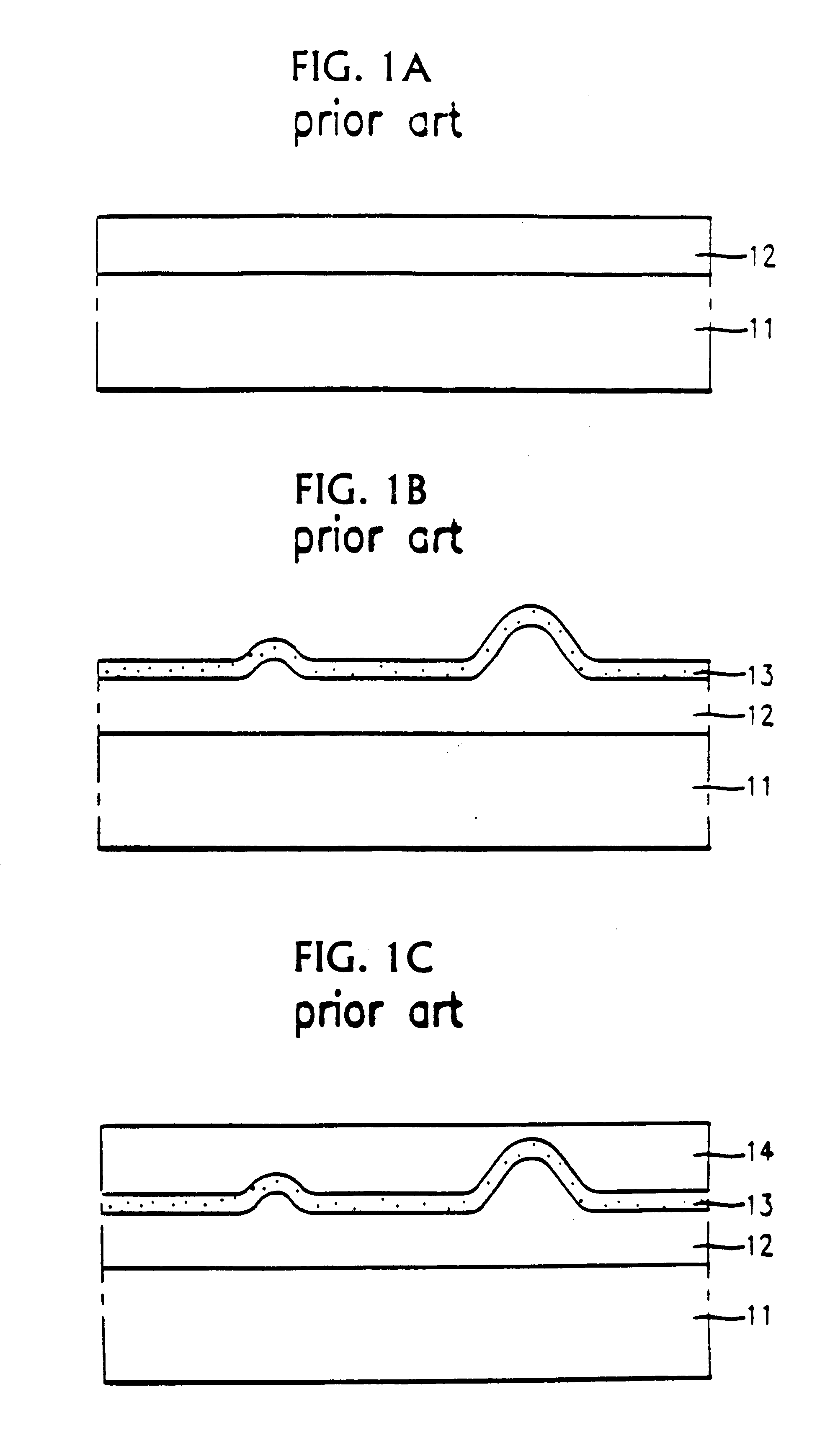
Reference will now be made in detail to the preferred embodiments of the present invention, examples of which are illustrated in the accompanying drawings.

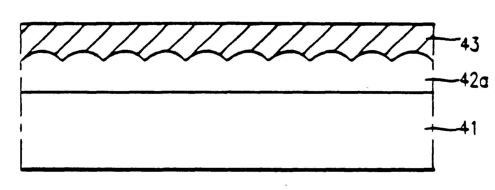
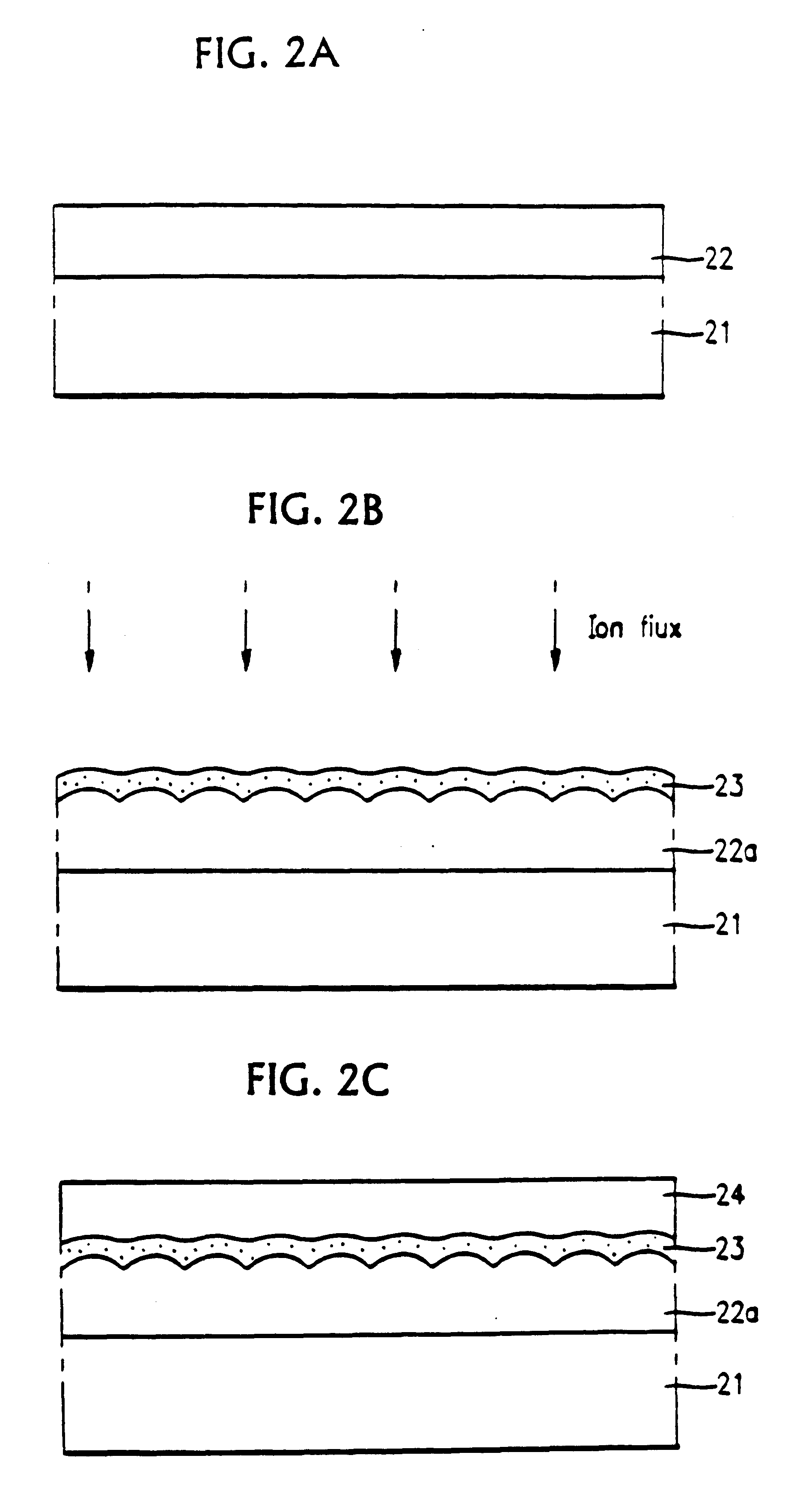
Referring to FIG. 2A, a first Pt layer 22 for a lower electrode of a capacitor is formed on a semiconductor substrate 21. Here, the first Pt layer 22 is formed at an ambient temperature. As shown in FIG. 2B, in order to generate uniform hillocks on the surface of the first Pt layer 22, external atoms are bombarded on the first Pt layer 22. In this process, hillocks are formed uniformly by inducing the stress at the first Pt layer 22.

Here, the bombardment of the external atoms on the first Pt layer is carried out by exposing the first Pt layer 22 to an Ar plasma. Then, a negative bias is applied thereto to collide Ar ions against the first Pt layer 22. Alternatively, the first Pt layer is exposed to an oxygen plasma to collide oxygen ions against the first Pt layer. In either way, hillocks are formed in uniform fashion on the first...


PUM


Abstract

A method of forming metal thin film of a memory device includes the steps of forming a metal layer on a semiconductor substrate, forming uniform grains on a surface of the metal layer, and forming a dielectric layer on the metal layer.

Description

This application claims the benefit of Korean Patent Application No. 48003 / 1996 filed Oct. 24, 1996, which is hereby incorporated by reference.1. Field of the InventionThe present invention relates to a method of forming a semiconductor device, and more particularly, to a method of forming a metal thin film. Although the present invention is suitable for a wide scope of applications, it is particularly suitable for forming a metal thin film used for a lower electrode in a high density memory device.2. Discussion of the Related ArtGenerally, a capacitor of a higher integrated DRAM is fabricated using a dielectric layer having a higher dielectric constant. However, if the dielectric layer is directly deposited on a polysilicon layer, the dielectric layer can easily react with silicon in the polysilicon layer. The reaction between the dielectric layer and the silicon eventually deteriorates an electrical characteristic of the capacitor.To avoid such a problem, lower and upper electrode...

Claims


Application Information

Patent Timeline
IPC IPC(8): H01L21/02H01L21/44H01L21/8247H01L21/28H01L21/822H01L21/8242H01L21/8246H01L27/04H01L27/10H01L27/105H01L27/108H01L29/788H01L29/792
CPCH01L28/84H01L28/65H01L27/1085Y10S438/937H10B12/03H01L21/28
Inventor JOO, JAE-HYUN
Owner TOW HOOK CONCEPTS
Why Eureka
Try Eureka