Method to optimize net lists using simultaneous placement and logic optimization

a logic optimization and net list technology, applied in the field of simultaneous placement and logic optimization, can solve problems such as loss of optimality, and achieve the effect of optimizing signal timing and circuit performan

Inactive Publication Date: 2003-02-18
SYNOPSYS INC
View PDF10 Cites 7 Cited by
  • Summary
  • Abstract
  • Description
  • Claims
  • Application Information

AI Technical Summary

Benefits of technology

Invention discloses a method for the design and fabrication of integrated circuits to optimize signal timing and circuit performance.

Problems solved by technology

Furthermore, mapping this solution into a valid placement and a valid implementation of each logic function can lead to loss of optimality.

Method used


Image

  • Method to optimize net lists using simultaneous placement and logic optimization
  • Method to optimize net lists using simultaneous placement and logic optimization
  • Method to optimize net lists using simultaneous placement and logic optimization

Examples


Embodiment Construction

)

Preferred embodiment is a method to simultaneously obtain a placement of logic functions wherein a logic function is an electrical circuit including logic gates and memory devices, mapping of logic functions onto library elements and buffering of nets to optimize timing in integrated circuits. Preferred embodiment is based on the Fidducia-Mattheyses optimization algorithm. Other optimization algorithms that are known in the art, such as simulated annealing and genetic algorithms, for example, could be used without deviating from the invention.

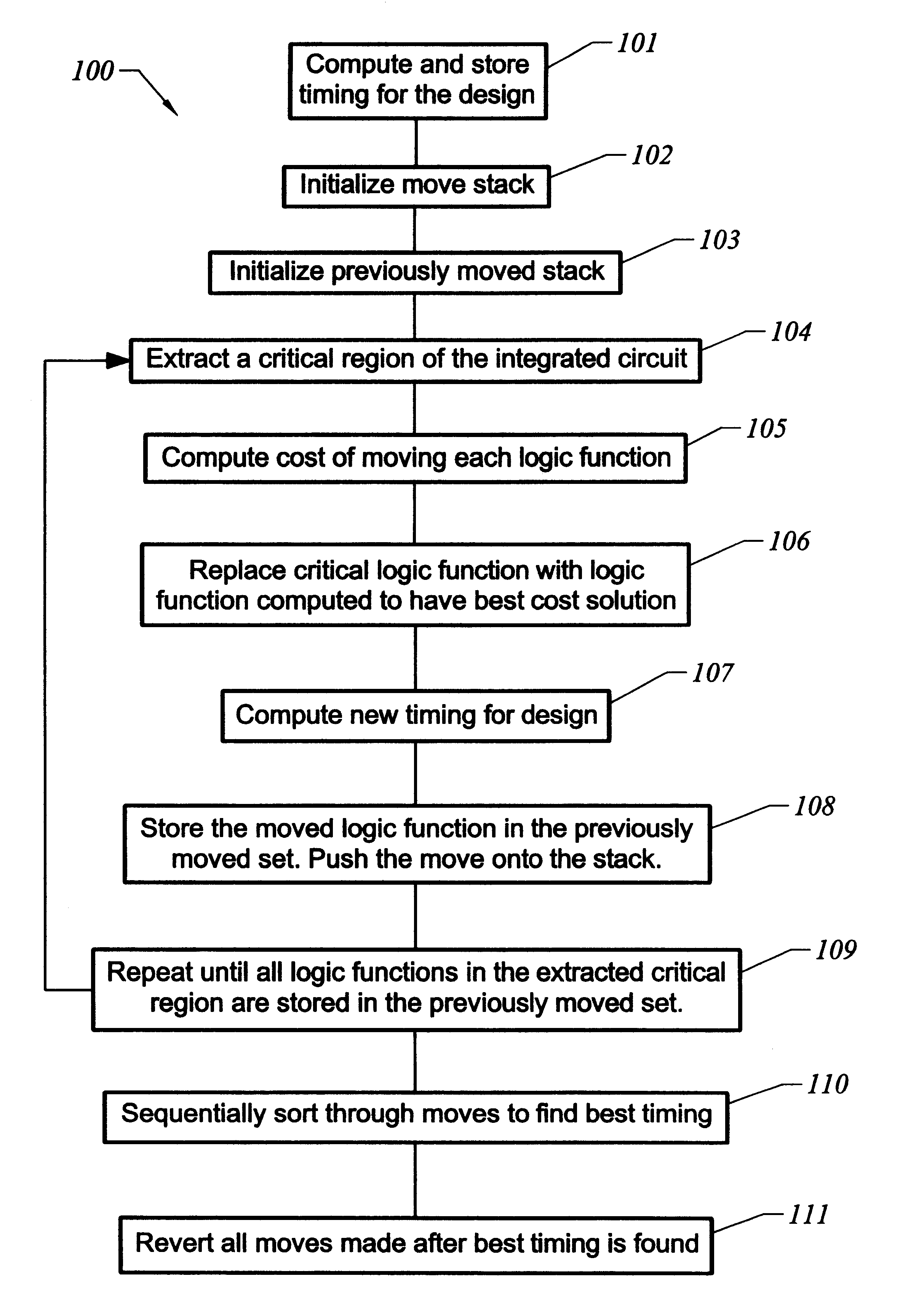
Method 100 consists of the following steps as shown in FIG. 7:

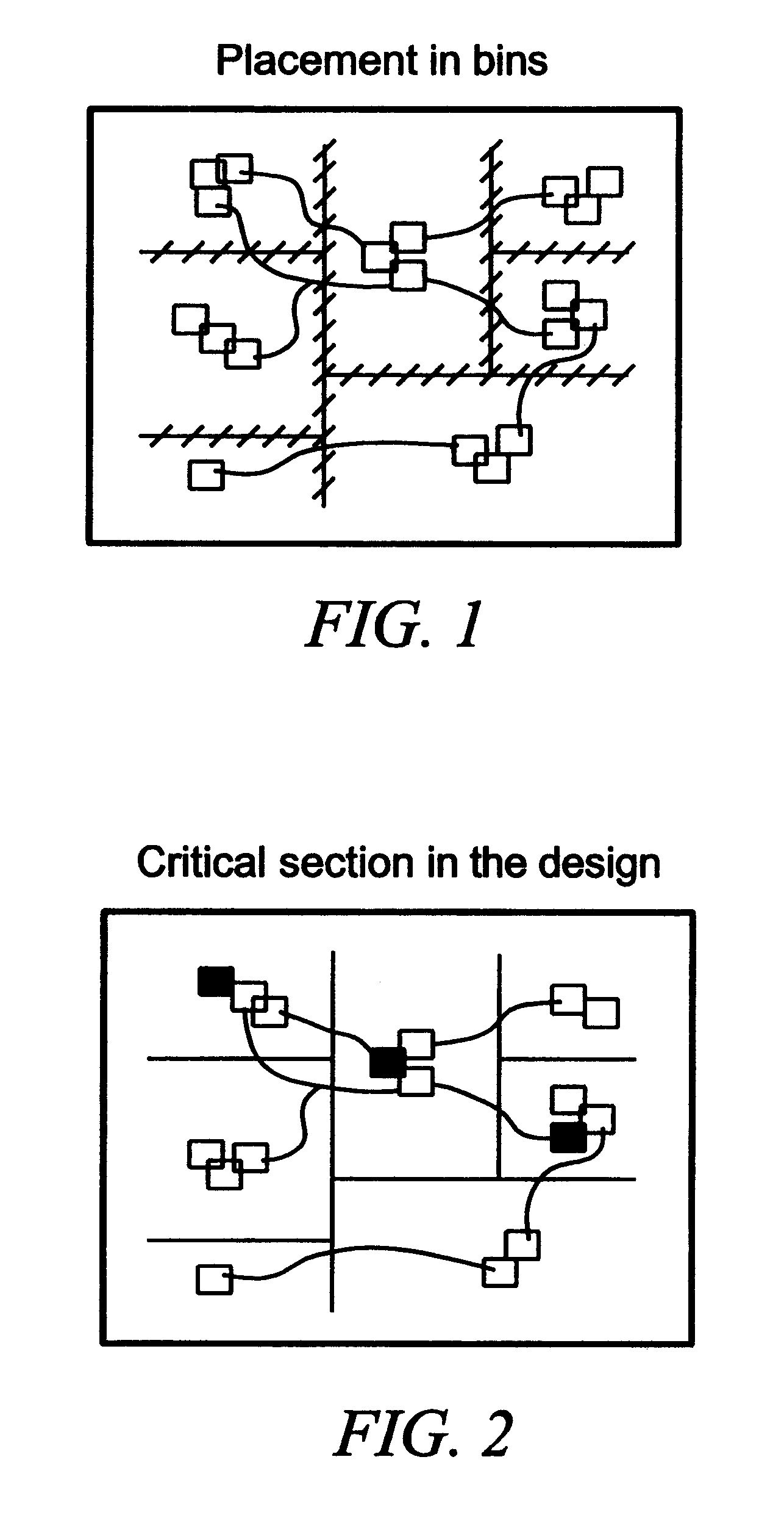
1. Compute and store timing for the design 101. A preliminary circuit is created to accomplish desired function of an integrated circuit. Timing information for each of the logic functions in the circuit is computed and stored to provide a base-line for subsequent attempts to reduce signal timing. FIG. 1 shows a possible initial configuration for the design. Possible locations are g...


PUM


Abstract

Method to optimize net lists used in the design and fabrication of integrated circuits by using simultaneous placement optimization, logic function optimization and net buffering algorithms. Method simultaneously obtains a placement of logic functions, mapping of logic functions on to library elements and buffering of nets connecting the logic functions.

Description

Invention relates to design of integrated circuits and more particularly to a method for optimizing net lists using simultaneous placement optimization, logic function optimization and net buffering.BACKGROUND OF INVENTIONPrior art methods use a mathematical expression to provide an analytical solution for simultaneous placement of logic functions and logic optimization. The solution of such a mathematical expression would lie in the continuous domain. Furthermore, mapping this solution into a valid placement and a valid implementation of each logic function can lead to loss of optimality.Therefore, there is a need for a method that will overcome the deficiencies found in the prior art.SUMMARY OF INVENTIONInvention discloses a method for the design and fabrication of integrated circuits to optimize signal timing and circuit performance.The method simultaneously obtains a placement of logic functions, mapping of logic functions onto library elements and buffering of nets connecting t...

Claims


Application Information

Patent Timeline
Patent Type & Authority Patents(United States)
IPC IPC(8): G06F17/50
CPCG06F17/505G06F30/327
Inventor GOPALAKRISHNAN, PADMINIRAJE, SALIL
Owner SYNOPSYS INC
Why Eureka
Try Eureka