

Method of making infrared sensor with a thermoelectric converting portion
- Summary
- Abstract
- Description
- Claims
- Application Information
AI Technical Summary
Problems solved by technology
Method used
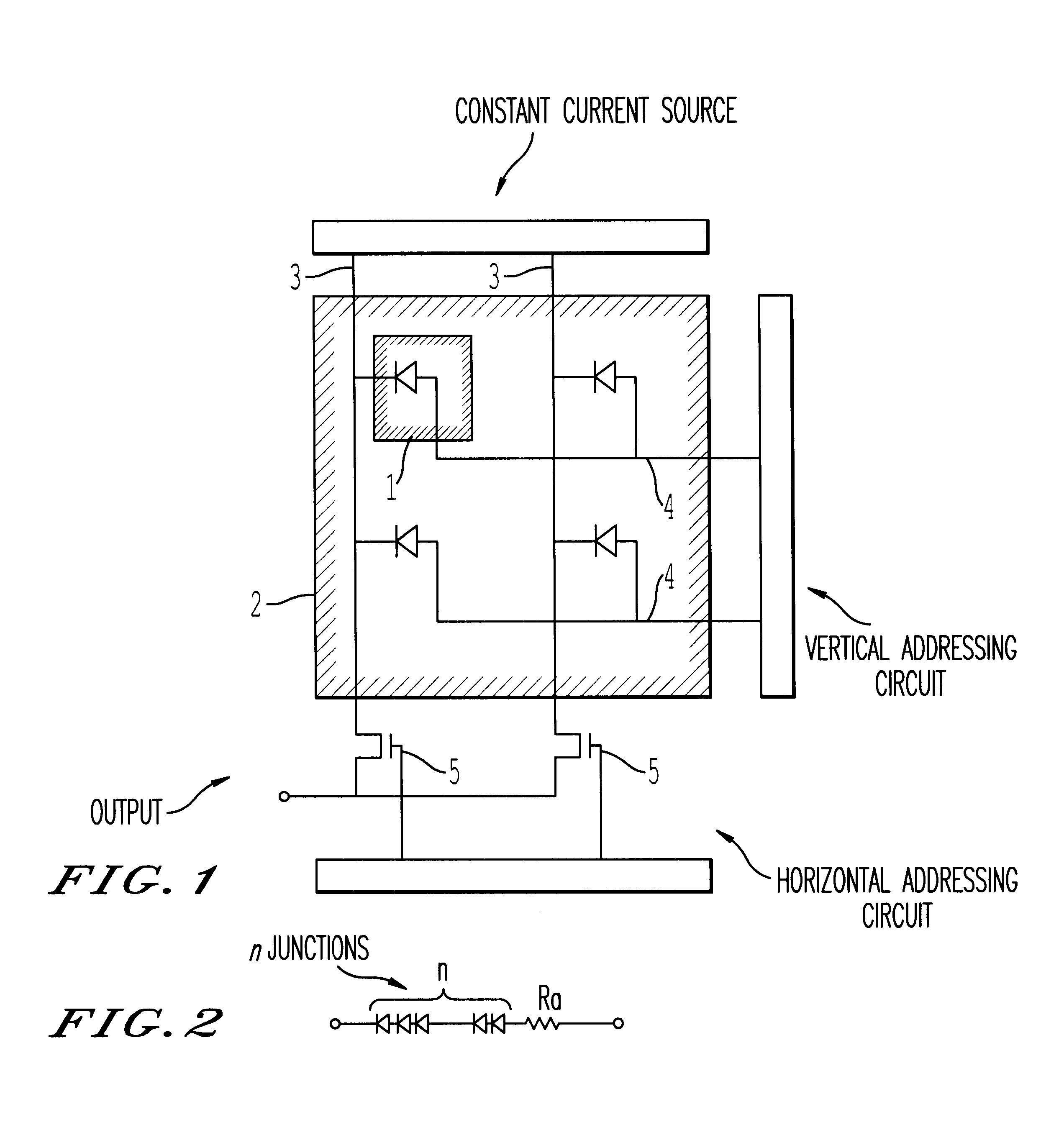
Image

Examples
first embodiment
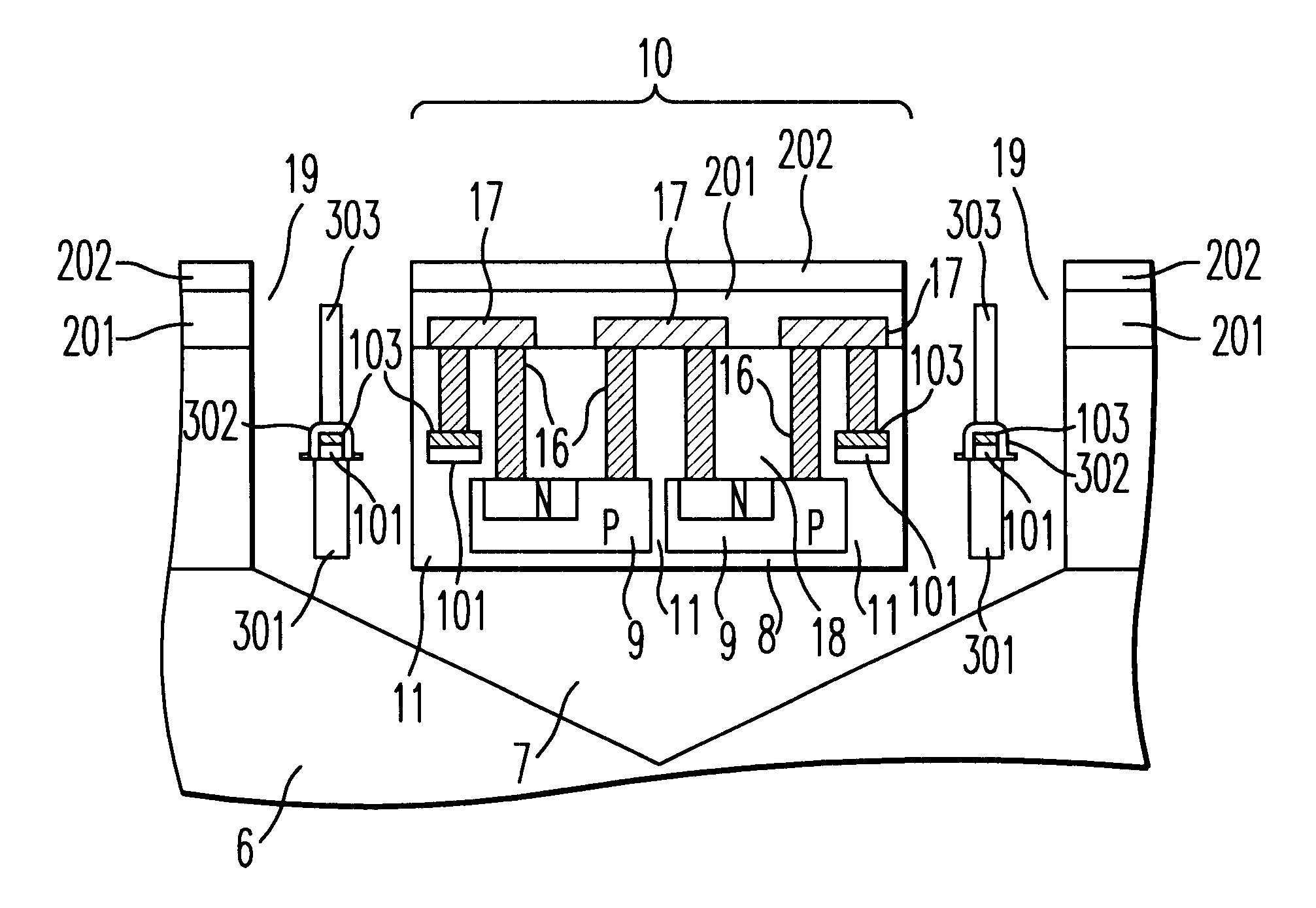
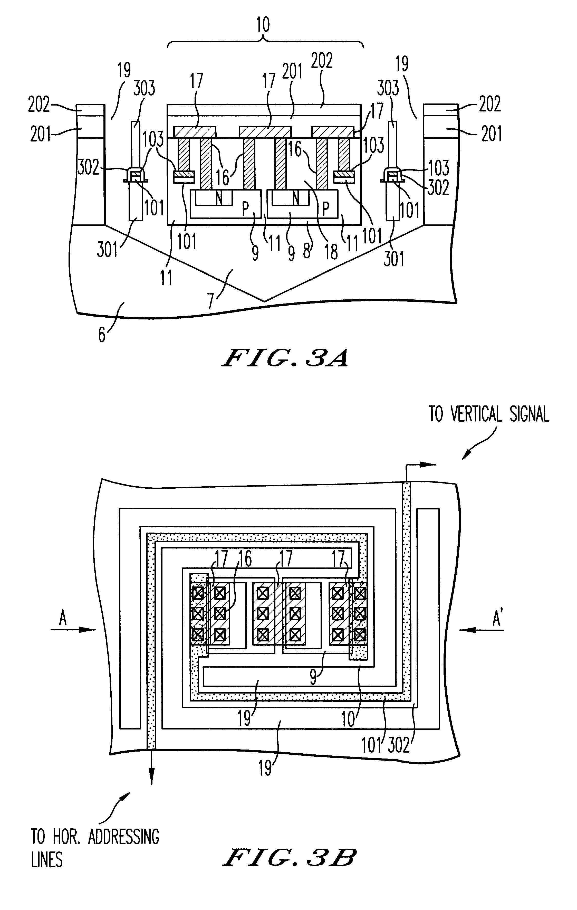
FIGS. 7A-9E are views illustrating steps for fabricating an infrared sensor in accordance with the present invention. The cross-sectional structures of MOS transistors in the peripheral circuitry and support structures are also shown in the same way as in FIGS. 4 and 5. The bonding pad is formed in the conductive interconnect layer lying immediately over the source / drain regions. Of course, other structures can also be adopted.
In the present embodiment, only one conductive interconnect (metallization) layer 17 is formed as shown in FIGS. 7A-9E. Of course, it is possible that multilayer metallization is formed, and the top metallization layer is used as a bonding pad.
First, the silicon nitride film 202 and the silicon oxide film 201 are etched by RIE to form a bonding pad opening 401 (FIG. 7A). The reason why the bonding pad opening 401 is formed prior to anisotropic etching of silicon for formation of a hollow structure as described later is that it is difficult to apply a resist us...
second embodiment
A second embodiment of the present invention is next described.
FIGS. 7A-9F are views illustrating process steps for fabricating an infrared sensor in accordance with the second embodiment of the invention. Cross-sectional structures of MOS transistors in the peripheral circuitry and of support structures are also shown in the same way as in FIGS. 4 and 5. A bonding pad is formed in a conductive interconnect layer located immediately over the source / drain regions. Of course, other structures may also be adopted.
In the present embodiment, one layer of metallization, or conductive interconnects, 17 is formed as shown in FIGS. 7A-9F. Obviously, multilayer metallization may be formed, and the top metallization layer may be used as a bonding pad.
In the present embodiment, process steps of FIGS. 7A-9F are exactly the same with their counterparts of the first embodiment described previously. Therefore, description of these steps is omitted. The final structure of the first embodiment is sho...
third embodiment
A method of fabricating an infrared sensor in accordance with a third embodiment of the present invention is next described by referring to FIGS. 11A-12D. The description will center on process steps carried out before and after the step of etching silicon.
FIGS. 11A-12D are views illustrating steps for fabricating the infrared sensor in accordance with the third embodiment of the invention. Cross-sectional structures of MOS transistors in the peripheral circuitry and of support structures are also shown in the same way as in FIGS. 4 and 5. A bonding pad is formed in a conductive interconnect layer located immediately over the source / drain regions. Of course, other structures may also be adopted.
In the present embodiment, only one layer of metallization, or conductive interconnects, 17 is formed as shown in FIGS. 11A-12D. Of course, multilayer metallization may be formed, and the top metal layer may be used as a bonding pad.
First, a silicon nitride film 202 and a silicon oxide film 2...
PUM
 Abstract
Description
Claims
Application Information