
Method for self-aligned shallow trench isolation and method of manufacturing non-volatile memory device comprising the same

a non-volatile memory and shallow trench technology, applied in the direction of semiconductor devices, basic electric elements, electrical apparatus, etc., can solve the problems of limited layout scalability, limited alignment tolerance, and isolation structure between individual cells within memory cell arrays

Inactive Publication Date: 2003-04-15
SAMSUNG ELECTRONICS CO LTD
View PDF6 Cites 52 Cited by
  • Summary
  • Abstract
  • Description
  • Claims
  • Application Information

AI Technical Summary

Problems solved by technology

Below the half-micron design rule, scalability of the layout is limited by photolithographic resolution attainable during manufacturing and by alignment tolerances of masks used during production.
Alignment tolerances are, in turn, limited by mechanical techniques employed to form masks and the techniques use to register these masks between layers.
Isolation structures between individual cells within the memory cell array consume regions of the chip that are otherwise useful for active circuitry.
However, their process of formation and / or the alignment of the structures generally dictate the size of the isolation structure.
This phenomenon is undesirable because it degrades the electrical characteristics of the memory device.
As such, alignment errors associated with forming the isolation structure and memory cells aggregate to induce mis-alignment, which may result in failure of the device.
Meanwhile, the bottom edge portion of the lower portion of the first polysilicon layer pattern 14 is bent outward to have a positive slope, which is eroded by an etchant introduced from above the substrate in the same manner as in the sidewall of a mesa structure or to act as a stopping layer of the underlying layer when the etchant is applied, which is undesirable.
This polysilicon residue 14a forms an electrical bridge between adjacent floating gates, which causes an electrical failure of the device.

Method used


Image

  • Method for self-aligned shallow trench isolation and method of manufacturing non-volatile memory device comprising the same
  • Method for self-aligned shallow trench isolation and method of manufacturing non-volatile memory device comprising the same
  • Method for self-aligned shallow trench isolation and method of manufacturing non-volatile memory device comprising the same

Examples


Embodiment Construction

Hereinafter, preferred embodiments of the present invention are described with reference to the accompanying drawings. Whenever a layer, structure, or pattern is described herein as being on, lying over, or covering another layer, pattern, or structure, it is meant that an interceding layer, pattern, or structure may or may not be included.

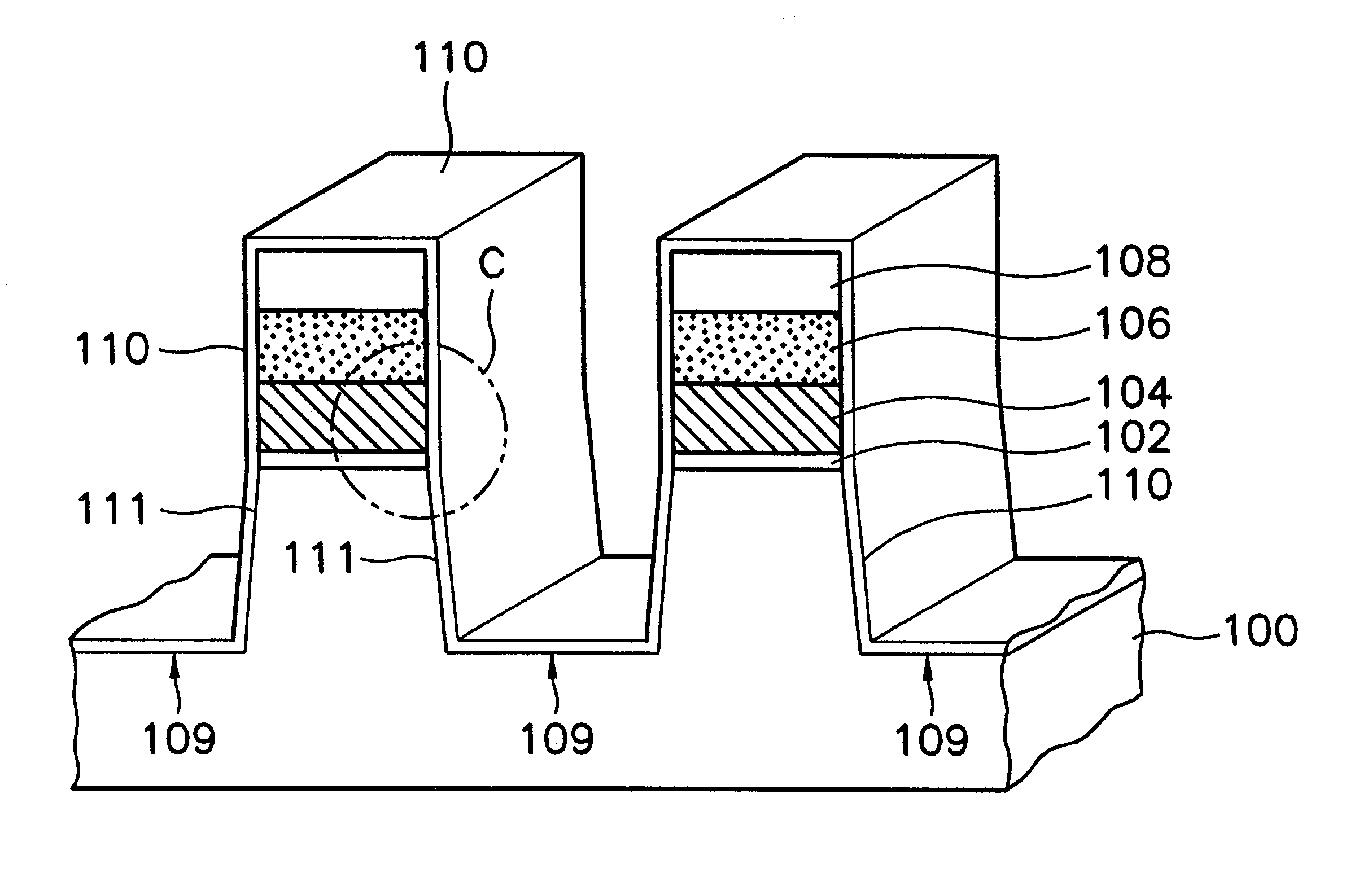
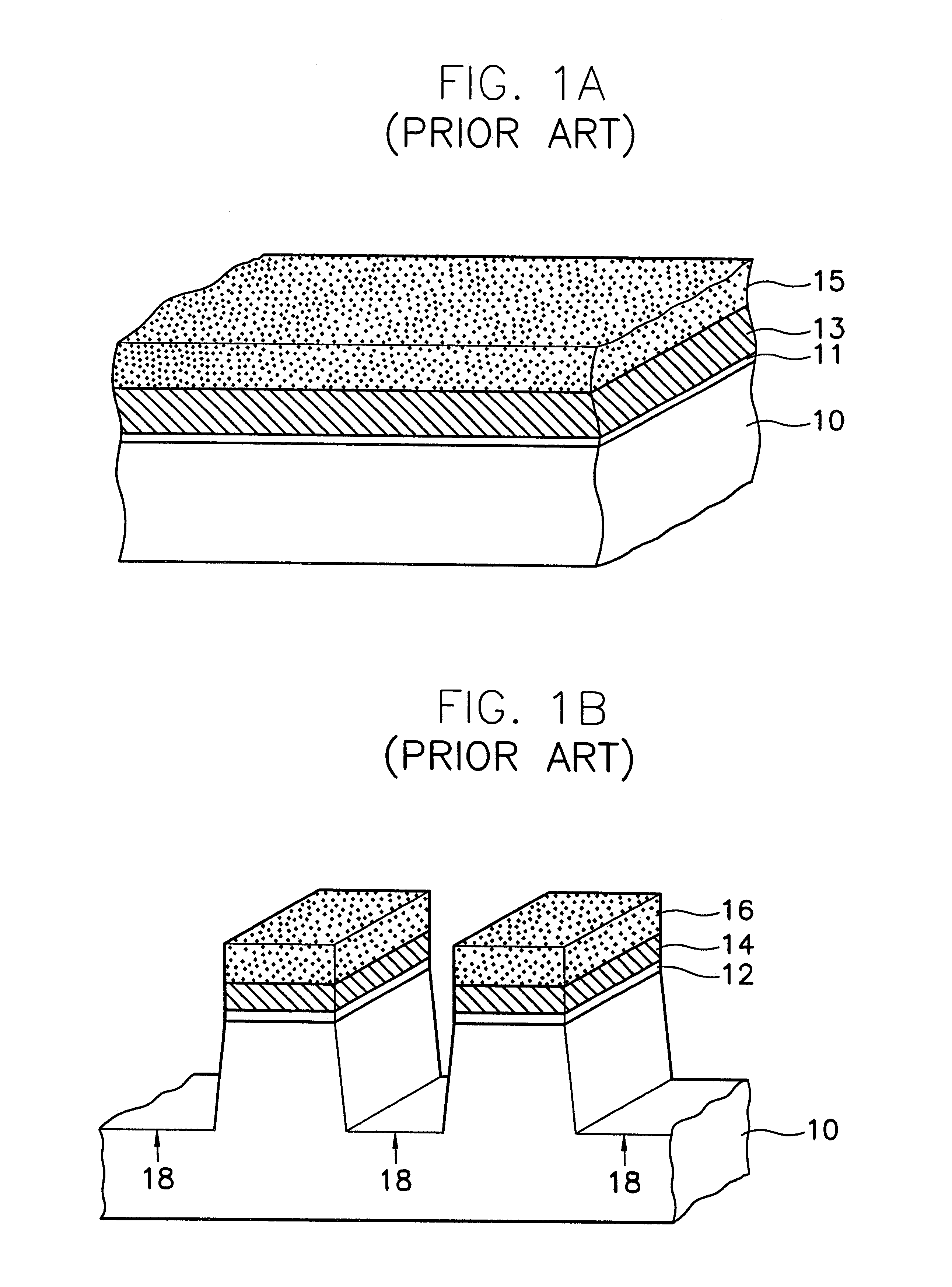
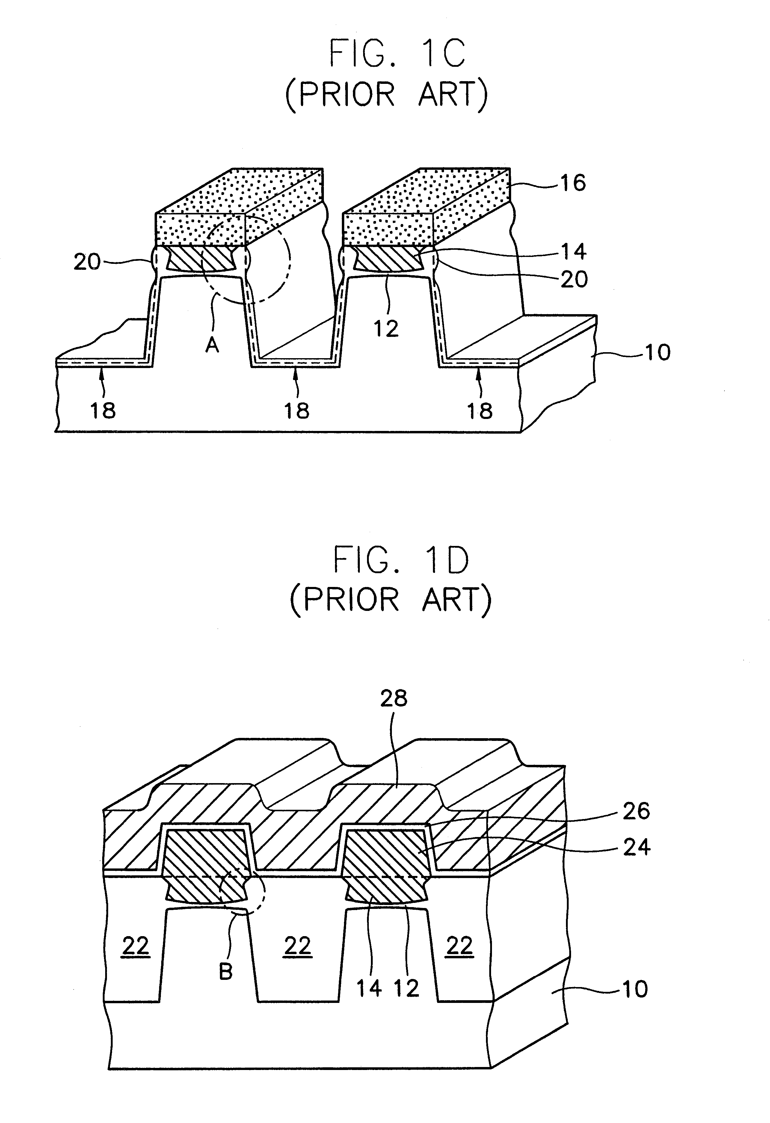
FIGS. 3A to 3H are perspective views illustrating a method of manufacturing a non-volatile memory device using a self-aligned shallow trench isolation process according to the present invention. Referring to FIG. 3A, a silicon oxide layer or silicon oxynitride layer is grown on a semiconductor substrate 100 comprising a material such as silicon, to form an oxide layer 101 which is to be used as a gate oxide layer (e.g., tunnel oxide layer) of a cell transistor. A polysilicon layer or an amorphous silicon layer is deposited on the oxide layer 101 to a thickness of about 300 to 1000 .ANG. via the LPCVD method. Then, the layer is doped with a high-co...


PUM

PropertyMeasurementUnit
temperatureaaaaaaaaaa
thicknessaaaaaaaaaa
thicknessaaaaaaaaaa

Abstract

A method of self-aligned shallow trench isolation and a method of manufacturing a non-volatile memory using the same are disclosed. An oxide layer, a first conductive layer and a nitride layer are successively formed on a semiconductor substrate. By using a single mask, the nitride layer, the first conductive layer and the oxide layer are etched to form an oxide layer pattern, a first conductive layer pattern and a nitride layer pattern. Subsequently, the upper portion of the substrate adjacent to the first conductive layer pattern is etched to form a trench. A CVD-oxide layer is deposited on the inner surface of the trench to form a trench inner-wall oxide layer, thereby preventing the formation of a positive profile at the sidewalls of the first conductive layer pattern. The trench inner-wall oxide layer is annealed in an N2O or NO atmosphere to form an oxynitride layer at the interface between the substrate and trench inner-wall oxide layer. Finally, a field oxide layer that fills up the trench is formed. Because the trench inner-wall oxide layer is formed by a CVD method to prevent the sidewalls of the first conductive layer pattern from having positive slopes, a conductive residue does not remain during a subsequent gate etching process.

Description

1. Field of the InventionThe present invention relates to an isolation method and a method of manufacturing a semiconductor device comprising the same. More particularly, the present invention relates to a self-aligned shallow trench isolation (SA-STI) technique that simultaneously forms a gate and an active region, and a method of manufacturing a non-volatile memory device comprising the same.2. Description of the Related ArtDuring the manufacture of memory devices, the packing density of cells is primarily determined by the layout of cells within the array and the physical dimensions of the cells themselves. Below the half-micron design rule, scalability of the layout is limited by photolithographic resolution attainable during manufacturing and by alignment tolerances of masks used during production. Alignment tolerances are, in turn, limited by mechanical techniques employed to form masks and the techniques use to register these masks between layers. Because alignment errors acc...

Claims


Application Information

Patent Timeline
Patent Type & Authority Patents(United States)
IPC IPC(8): H01L21/762H01L21/70H01L27/115H01L21/8234H01L21/8247H10B69/00
CPCH01L21/76224H01L27/11521H01L27/115H01L21/823481H10B69/00H10B41/30
Inventor CHUNG, BYUNG-HONG
Owner SAMSUNG ELECTRONICS CO LTD
Learn More