Residue-compensating A/D converter

a dc converter and adc technology, applied in the field of data conversion, can solve the problems of circuit electrical properties to drift, low reliability, and low availability of high-performance adcs for xdsl modems,

Inactive Publication Date: 2003-04-29
ANALOG DEVICES BV
View PDF3 Cites 119 Cited by
  • Summary
  • Abstract
  • Description
  • Claims
  • Application Information

AI Technical Summary

Problems solved by technology

The available high-performance ADCs needed for xDSL modems are relatively expensive and will often represent a large fraction of the system's overall cost.
Furthermore, considering that the required good linearity usually is achieved by brute-force calibration of the ADC circuit, the long-term performance reliability may be poor due to aging, ambient temperature variations, and other effects which may cause the circuit's electrical properties to drift.
Unfortunately, in doing so, the circuit's power consumption will also be increased by the same factor of 64.
Hence, increasing C.sub.DAC is not a very attractive way to improve the linearity, especially not for ADCs intended for use in battery-powered equipment.
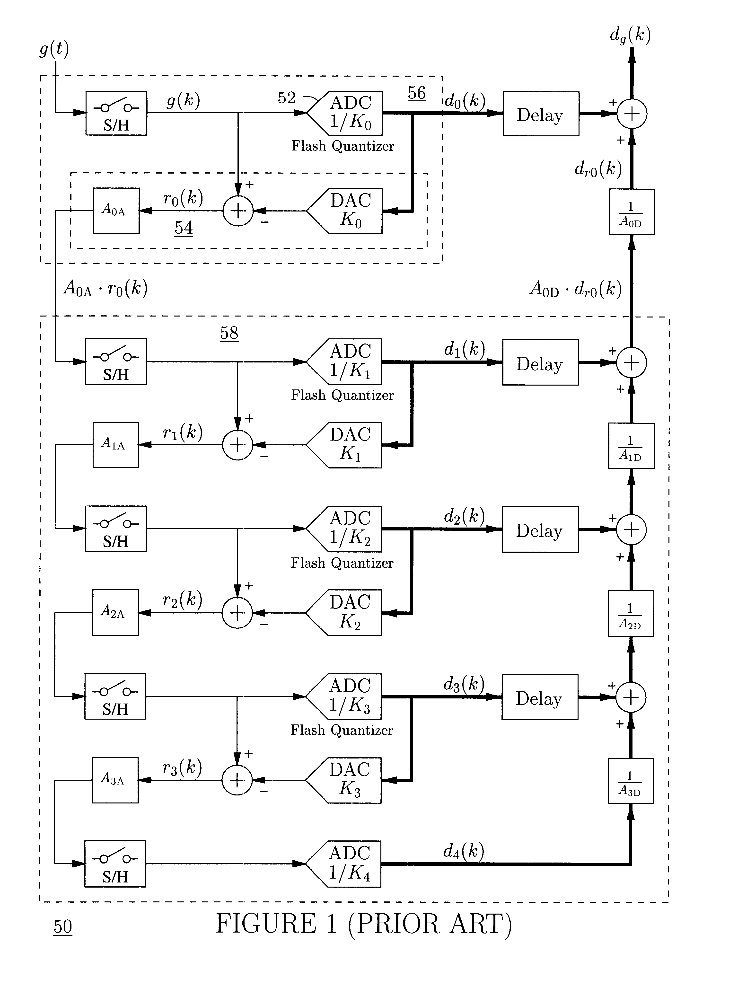
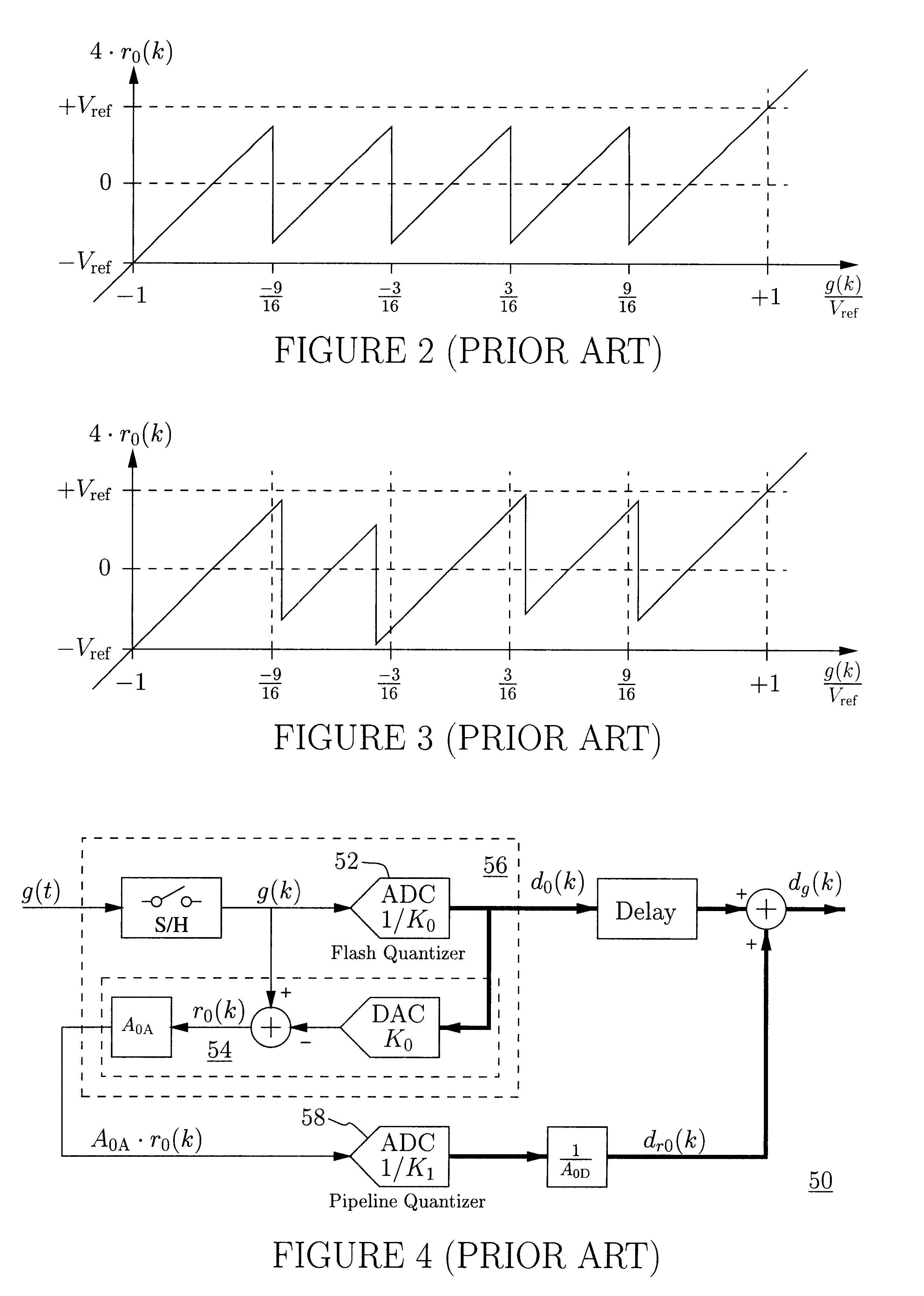
Mismatch of A.sub.0A and A.sub.0D (or equivalently, mismatch of K.sub.0 and K.sub.1) is another potential source of significant nonlinearities.

Method used


Image

  • Residue-compensating A/D converter
  • Residue-compensating A/D converter
  • Residue-compensating A/D converter

Examples


first embodiment

Consider FIG. 8, which shows a modified version [56A] of the pipeline ADC's [50] input stage [56]. The objective of the modified input stage [56A] is to uncorrelate from the input signal the errors caused by mismatch of the DAC capacitors [66], i.e., to convert distortion errors into a noise-like error signal. This objective is achieved by inserting a mismatch-shaping encoder [74] in between the flash quantizer [52] and the DAC's voltage buffer [64]. The mismatch-shaping encoder [74] merely interchanges the order of the four boolean values, x.sub.0, x.sub.1, x.sub.2, and x.sub.3, to generate another sequence, y.sub.0, y.sub.1, y.sub.2, and y.sub.3, of the same boolean values. In other words, y.sub.0 y.sub.1 y.sub.2 y.sub.3 is a permutation of x.sub.0 x.sub.1 x.sub.2 x.sub.3. The operation of permuting x.sub.0 x.sub.1 x.sub.2 x.sub.3 can, e.g., be performed by a rotating multiplexer circuit [76] shown in FIG. 9. The input sequence, x.sub.0 x.sub.1 x.sub.2 x.sub.3, is first rotated by...

second embodiment

ADC circuits produced in large volumes or employed in critical applications (medical, space, etc.) should preferably not rely on calibration and the power consumption should be minimal. These objectives can be achieved by using a first-order (instead of a zero-order) mismatch-shaping encoder [74] in the modified input stage [56A]. Several first-order mismatch-shaping encoders have been invented and disclosed in the past 10 years (see, e.g., the following U.S. Pat. No. 5,138,317 to Story, U.S. Pat. No. 5,221,926 to Jackson, U.S. Pat. No. 5,404,142 to Adams, and U.S. Pat. No. 5,684,482 to Galton). However, these encoders either suffer from an idle-tone problem (i.e., from mismatch-induced spurious tones, which are as undesirable as tones caused by harmonic distortion), or they have a poor spectral-shaping efficiency at high frequencies. A particularly simple, highly-efficient, and idle-tone-free family of mismatch-shaping encoders was described by Steensgaard in "Idle-Tone Free Mismat...

third embodiment

As discussed above concerning the first embodiment, errors representing themselves as spurious tones are generally significantly more deleterious than noise-like errors. It is, therefore, an objective to convert r.sub.0 (k) into a noise-like signal, whereby mismatch of the gain factor A.sub.0A will become much less of a problem. This objective can be achieved by dithering the flash quantizer [52] as shown in FIG. 17. The dithered flash quantizer [88] conceptually is implemented by adding a random signal p.sub.0 (k) to g(k), the sum of which is quantized by the flash quantizer [52]. The dithered quantizer [88] will nominally be absolutely linear, however noisy, if the random signal's p.sub.0 (k) probability is uniformly distributed in a range which is as wide as the difference between two of the flash quantizer's [52] neighboring threshold voltages. FIG. 18 shows how the dithered flash quantizer [88] can be implemented. Instead of directly adding p.sub.0 (k) to g(k), the negative of ...


PUM


Abstract

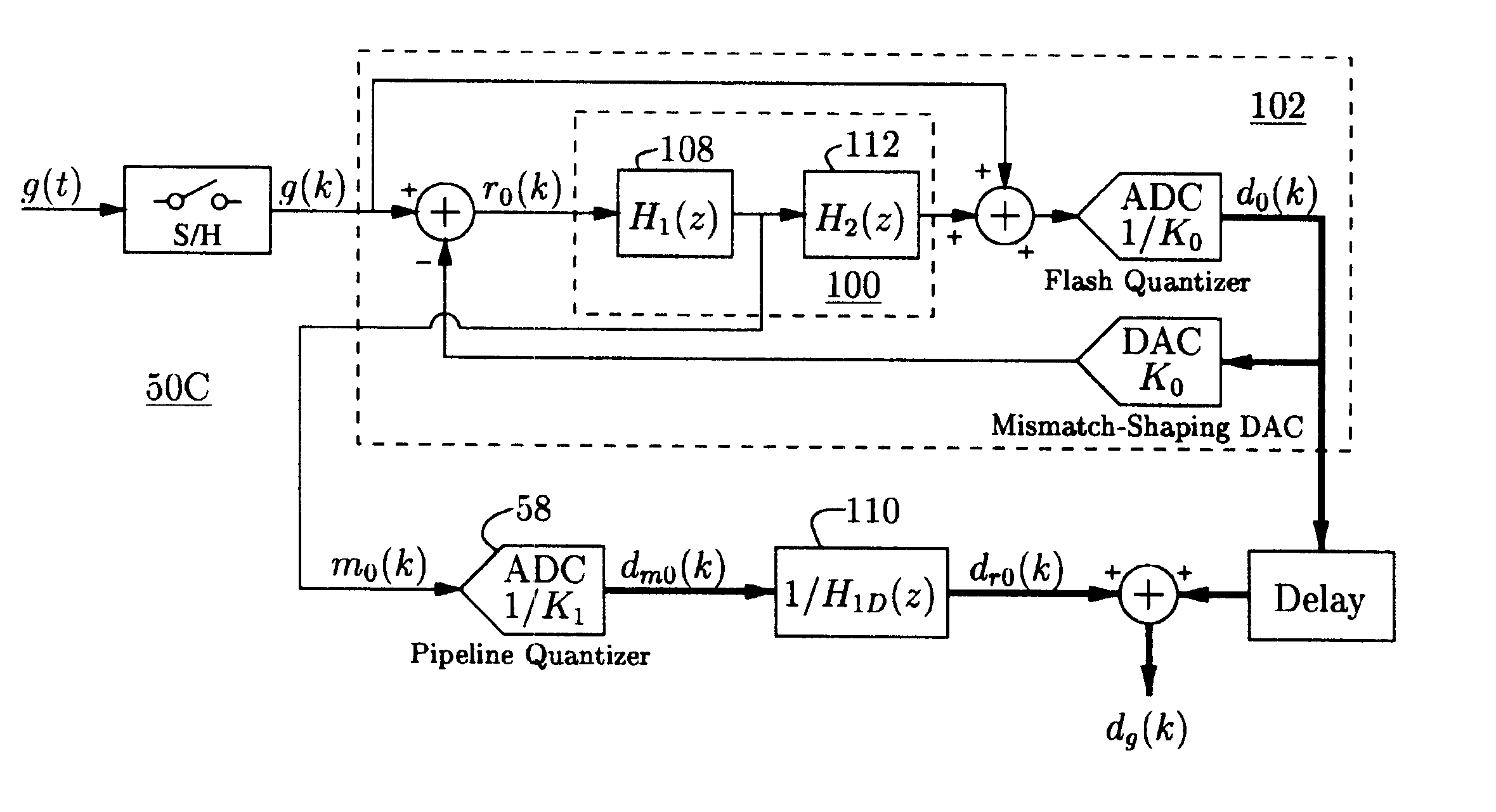
An analog-to-digital converter system [50D] processing an input signal, g, which can be either a discrete-time or a continuous-time signal. A first quantizer [154] generates a first digital signal, d0(k), representing the sum of the input signal, g, and a dithering signal, y0. A digital-to-analog converter [156] generates an analog feedback signal, alpha, representing accurately the first digital signal, d0(k). The DAC [156] may be linearized by the use of mismatch-shaping techniques. A filter [158] generates the dithering signal, y0, by selectively amplifying in the signal band the residue signal, r0, defined as the difference of the input signal, g, and the analog feedback signal, alpha. Optional signal paths [166][168] are used to minimize the closed-loop signal transfer function from g to y0, which ideally will be zero. An analog compensation signal, m0, which is described by a well-controlled relationship to the residue signal, r0, is extracted from the filter [158]. Ideally, the closed-loop signal transfer function from g to m0 will be zero, or at least small in the signal band. A second quantizer [160] converts the analog compensation signal, m0, into a second digital signal, dm0(k). The two digital signals, d0(k) and dm0(k), are filtered individually and then added to form the overall output signal, dg(k). The second digital filter [164] has a low signal-band gain, which implies that the sensitivity to signal-band errors caused by the second quantizer [160] will be low. The output signal, dg(k), is a highly-accurate high-resolution representation of the input signal, g. Circuit imperfections, such as mismatch, gain errors, and nonlinearities, will cause only noise-like errors having a very low spectral power density in the signal band.The invention facilitates the implementation of uncalibrated highly-linear high-resolution wide-bandwidth A/D converters [50D], e.g., for use in digital communication systems, such as xDSL modems and other demanding consumer-market products for which low cost is of the essence.

Description

1. FIELD OF INVENTIONThe field of invention is data conversion, more particularly, this invention relates to multi-step analog-to-digital converters.1.2 InventorJesper Steensgaard-Madsen, 448 Riverside Drive, apartment # 2, New York, N.Y. 10027, USA, is the sole inventor and applicant. The applicant is a citizen of Denmark.2. DESCRIPTION OF PRIOR ARTHighly-linear high-speed analog-to-digital converters (ADCs) are key elements in many electrical systems of great importance. Digital communication systems, e.g., digital-subscriber-line (xDSL) modems, which are capable of providing wide-bandwidth communication via traditional phone lines, are an example of where a system's overall performance may be limited by the ADC front-end's finite linearity. The available high-performance ADCs needed for xDSL modems are relatively expensive and will often represent a large fraction of the system's overall cost. Furthermore, considering that the required good linearity usually is achieved by brute-...

Claims


Application Information

Patent Timeline
Patent Type & Authority Patents(United States)
IPC IPC(8): H03M3/00H03M1/14H03M3/04
CPCH03M3/416H03M1/145
Inventor STEENSGAARD-MADSEN, JESPER
Owner ANALOG DEVICES BV
Why Eureka
Try Eureka