Light-emitting device
a technology of light-emitting devices and light-emitting films, which is applied in the direction of sustainable manufacturing/processing, instruments, and final product manufacturing, etc., can solve the problems of achieve the effect of reducing the deterioration of organic el films
- Summary
- Abstract
- Description
- Claims
- Application Information
AI Technical Summary
Benefits of technology
Problems solved by technology
Method used
Image
Examples
embodiment 1
will be explained with reference to FIGS. 3A to 5B. Note that shown in FIGS. 3A to 4D are cross sectional views of manufacturing processes in a pixel portion. Furthermore, the top view of a pixel formed in accordance with Embodiment 1 (a top view at the point of the formation of an anode) is shown in FIG. 5A, and a final circuit configuration of the pixel is shown in FIG. 5B. It is to be noted that the reference numerals used in FIGS. 5A and 5B correspond to those used in FIGS. 3A to 4D.
First, as shown in FIG. 3A, a glass substrate 301 is prepared as the element-forming substrate, and an insulating film 302 made of a silicon oxide film is formed thereon to a thickness of 200 nm. The insulating film 302 may be formed by employing low pressure thermal CVD, plasma CVD, sputtering, or evaporation.
A crystalline silicon film 303 is next formed to a thickness of 50 nm on the insulating film 302. A known method may be used as the formation method of the crystalline silicon film 303. An amor...
embodiment 2
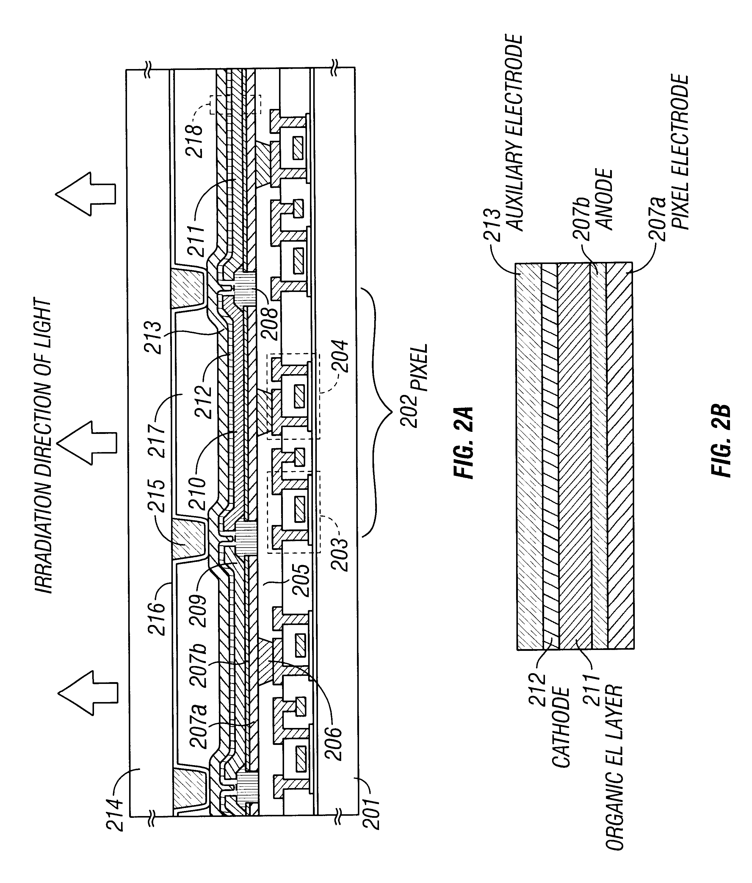
In Embodiment 2, an explanation will be made with reference to FIG. 6 on an EL light-emitting device having a pixel with a structure that is different from that of the EL light-emitting device shown in FIG. 2. Note that in Embodiment 2, the structure of the EL light-emitting device may be manufactured by adding a few changes to the structure of FIG. 2, and hence explanations will be made on the points that are different from those of FIG. 2. Therefore, the embodiment mode may be referenced concerning the explanation of the parts that are denoted by the same reference numerals with those of FIG. 2.
In Embodiment 2, upon forming a contact hole in the interlayer insulating film 205, a pixel electrode 601a and an anode 601b are formed in this state. Then, an insulating film 602 is formed to fill up the concave portion formed by the contact hole. The insulating film 602 is called a filling-up insulating film in Embodiment 2. The filling-up insulating film 602 can be formed at the same tim...
embodiment 3
Although only the structure of the pixel portion is shown in the EL light-emitting device illustrated in Embodiment 1, a driver circuit for driving the pixel portion may be formed integrally therewith on the same substrate. When forming the driver circuit, the driver circuit may be formed of an nMOS circuit, a pMOS circuit, or a CMOS circuit. Of course, only the pixel portion may be formed of a TFT, and a driver circuit containing an IC chip may be used as an external-attached driver circuit.
Further, the manufacturing processes in Embodiment 1 are reduced by forming the pixel portion with the P channel TFT only. However, in case of Embodiment 2, the driver circuit is formed of the pMOS circuit, and a driver circuit containing an IC chip can be used as the driver circuit that cannot be formed of the pMOS circuit.
Note that the constitution of Embodiment 2 may be implemented by freely combining it with the constitution of Embodiment 1 or 2.
PUM
 Abstract
Description
Claims
Application Information


