Magnetic sensor device

a magnetic sensor and sensor technology, applied in the field of magnetic sensor devices, can solve the problems of gmr sensor being a sensor disadvantageous, no sensor can meet a request to the magnetic sensor, and reaching the limit of the capacity to keep and develop the part of the magnetic sensor

Inactive Publication Date: 2003-05-20
SUGITANI NOVUYOSHI
View PDF2 Cites 115 Cited by
  • Summary
  • Abstract
  • Description
  • Claims
  • Application Information

AI Technical Summary

Problems solved by technology

However, the prior arts have reached the limit of the capability to keep and develop the part of the magnetic sensor in the future, and therefore the technology of speeding up processing requires the development of a magnetic sensor device based on a new principle capable of speeding up processing.
However, none of the sensors can yet meet a request to the magnetic sensor, such as the speedup of processing incident to the processing of a rapidly increasing amount of information.
This shows that the GMR sensor is a sensor disadvantageous for detection of a change in high frequencies of the magnetic field to be detected.
Causes of output hysteresis include hysteresis of magnetic properties (a B-H curve) of a magnetic material, and magnetic aftereffect.
Because of these magnetic loss phenomena, there is a threshold frequency which does not change with an external magnetic field and cannot be detected.
A more suitable material for high frequencies is prone to reduce an absolute value of impedance, and it is, in general, very difficult to form a circuit configuration for detecting the amount of change in impedance at high frequencies.
Therefore, the MI device is not suitable for a smaller size and higher frequencies.
When a magnetic material is being magnetized through the application of a high-frequency alternating field to the magnetic material, various losses increase as the frequency of the applied alternating field increases.
These losses are caused by phase delay resulting from a phenomenon in which a magnetic flux generated by the magnetization of the magnetic material cannot keep up with a change in the alternating field.
The application of an alternating field to a magnetic material at high frequencies causes the occurrence of various losses.
Firstly, a hysteresis loss is a loss which occurs at the lowest frequency.
Secondly, it is an eddy current loss that becomes a problem as the frequency becomes higher.
The eddy current loss is that an alternating field causes electromagnetic induction to generate an eddy current in a magnetic material, and the current passes through the magnetic material and changes into heat, which is thus consumed.
However, as the frequency increases, the movement of the spin cannot keep up with a change in the alternatin

Method used


Image

  • Magnetic sensor device
  • Magnetic sensor device
  • Magnetic sensor device

Examples


second example

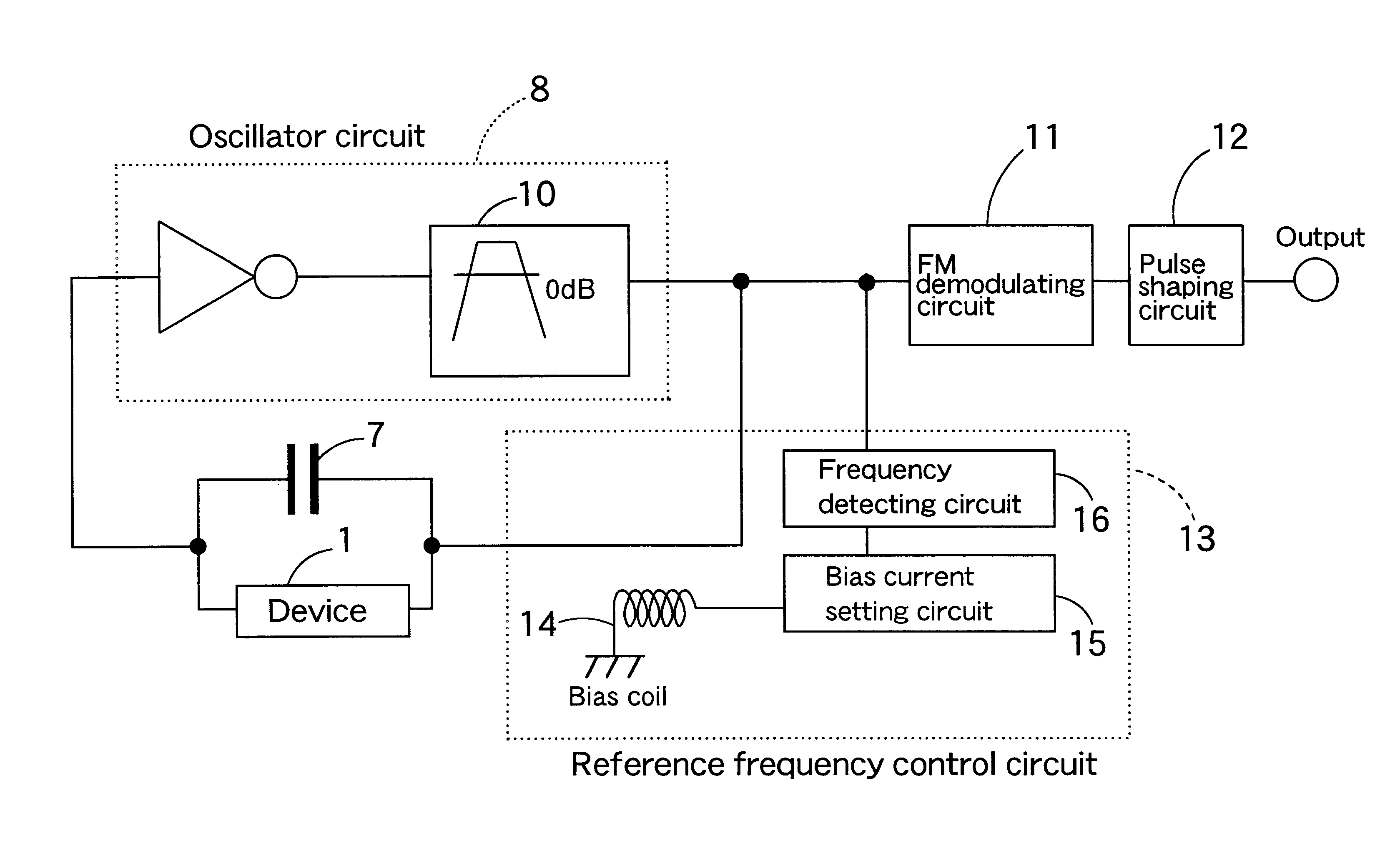
FIG. 24 shows a magnetic sensor device of a second example. In the second example, the above-described bias magnetic field generator device 36 and thin film magnetic sensor 31 are formed on the same semiconductor substrate (a silicon wafer) 39. A capacitor 47 to be connected to the thin film magnetic sensor 31, an oscillator circuit 48, and a reference frequency control circuit 43 to be connected to the bias magnetic field generator device 36 are also formed on the same semiconductor substrate 39. An FM demodulating circuit 44 to be connected to an output of the oscillator circuit 48, a pulse shaping circuit 42 to be connected to an output side of the FM demodulating circuit 44, and a bias current control circuit 45 which detects the frequency of the oscillator circuit 48 through a frequency detector current 41 and controls the bias magnetic field generator device 36 are also formed on the same semiconductor substrate 39. The devices and the circuits are connected through a conducti...

third example

FIG. 25 shows a magnetic sensor device of a third example. In the third example, a magnetic film 53 of a thin film magnetic sensor 51 is made to be a single-layer film, and the magnetic film 53 is mounted on a conductive layer 32 with an insulating layer 34 in between. As described above, a multilayer magnetic film can reduce a loss incident to high frequencies, but the single-layer magnetic film 53 can be used as long as the magnetic film can have a high magnetic resonance frequency through appropriate selection of a material of the magnetic film.

fourth example

FIG. 26 shows a magnetic sensor device of a fourth example. In the fourth example, a thin film magnetic sensor 51 has a structure in which a conductive layer 62 is sandwiched between insulating layers 65 and a magnetic film 63 is formed on a conductive layer 62 with the insulating layer 65 in between. This structure allows increasing the ratio of a reactance component of the magnetic sensor to a parasitic impedance, thereby making it easy that the oscillation conditions of the oscillator circuit hold.


PUM


Abstract

A magnetic sensor device has a magnetic sensor having a magnetic material whose threshold frequency is changed by a magnetic field to be detected, and the device has the so-called electromagnetically-coupled current path which is affected by the magnetic material in order to electrically detect the threshold frequency of the magnetic material. The current path is connected to an oscillator circuit, which is set so that its oscillation frequency is changed by a change in the threshold frequency of the magnetic sensor. In the magnetic sensor device, the magnetic field to be detected causes a change in the oscillation frequency of the oscillator circuit, and the change in the frequency is extracted as a magnetic field detection signal. More specifically, a change in the threshold frequency of the magnetic material of the magnetic sensor caused by the magnetic field to be detected is extracted as a change in an output frequency of the oscillator circuit, and the change in the output frequency is used as the magnetic field detection signal.

Description

1. Field of the InventionThe present invention relates to a magnetic sensor device which detects a change in magnetic properties of a magnetic material caused by an external magnetic field by using an imaginary part of complex magnetic permeability of the magnetic material, that is, characteristics of a frequency range in which the magnetic material loses its own properties. More particularly, the present invention relates to a magnetic sensor device which is used to detect a magnetic pattern stored through magnetization, such as a magnetic head of a hard disk drive or the like, a rotary encoder for use in a motor or the like, or a magnetic head of a barcode reader, and which is used for a signal transmitter which transmits a signal through a magnetic field excited by an electric signal in a digital household electrical appliance such as a mobile telephone, a DVD (a digital versatile disc) or a digital television, or the like.2. Description of the Prior ArtRecent advances in microel...

Claims


Application Information

Patent Timeline
IPC IPC(8): G01R33/02G11B5/00G11B5/33
CPCG01R33/02G11B2005/0005G11B5/332
Inventor SUGITANI, NOVUYOSI
Owner SUGITANI NOVUYOSHI
Why Eureka
Try Eureka