Semiconductor apparatus with decoupling capacitor

a technology of capacitor and semiconductor, applied in the direction of electrical apparatus contruction details, cross-talk/noise/interference reduction, etc., can solve the problem of hard to reduce electromagnetic radiation noise generated in the semiconductor package, the power supply/ground noise inside the semiconductor package cannot be removed sufficiently, and the parasitic inductance is increased. problem, to achieve the effect of sufficiently reducing power supply/ground nois

Inactive Publication Date: 2003-08-19
LAPIS SEMICON CO LTD
View PDF15 Cites 63 Cited by
  • Summary
  • Abstract
  • Description
  • Claims
  • Application Information

AI Technical Summary

Benefits of technology

Accordingly, an object of the present invention is to provide a semiconductor apparatus in which power-supply / ground noise is sufficiently reduced.

Problems solved by technology

According to such a conventional semiconductor apparatus, the power supply / ground noise inside the semiconductor package cannot be removed sufficiently.
As a result, it is hard to reduce electromagnetic radiation noise generated in the semiconductor package.
Further, since a conductive route formed between the semiconductor package and the chip capacitor is long, parasitic inductance is increased.
And therefore, the chip capacitor does not effectively function to reduce the power supply / ground noise.

Method used


Image

  • Semiconductor apparatus with decoupling capacitor
  • Semiconductor apparatus with decoupling capacitor
  • Semiconductor apparatus with decoupling capacitor

Examples


first preferred embodiment

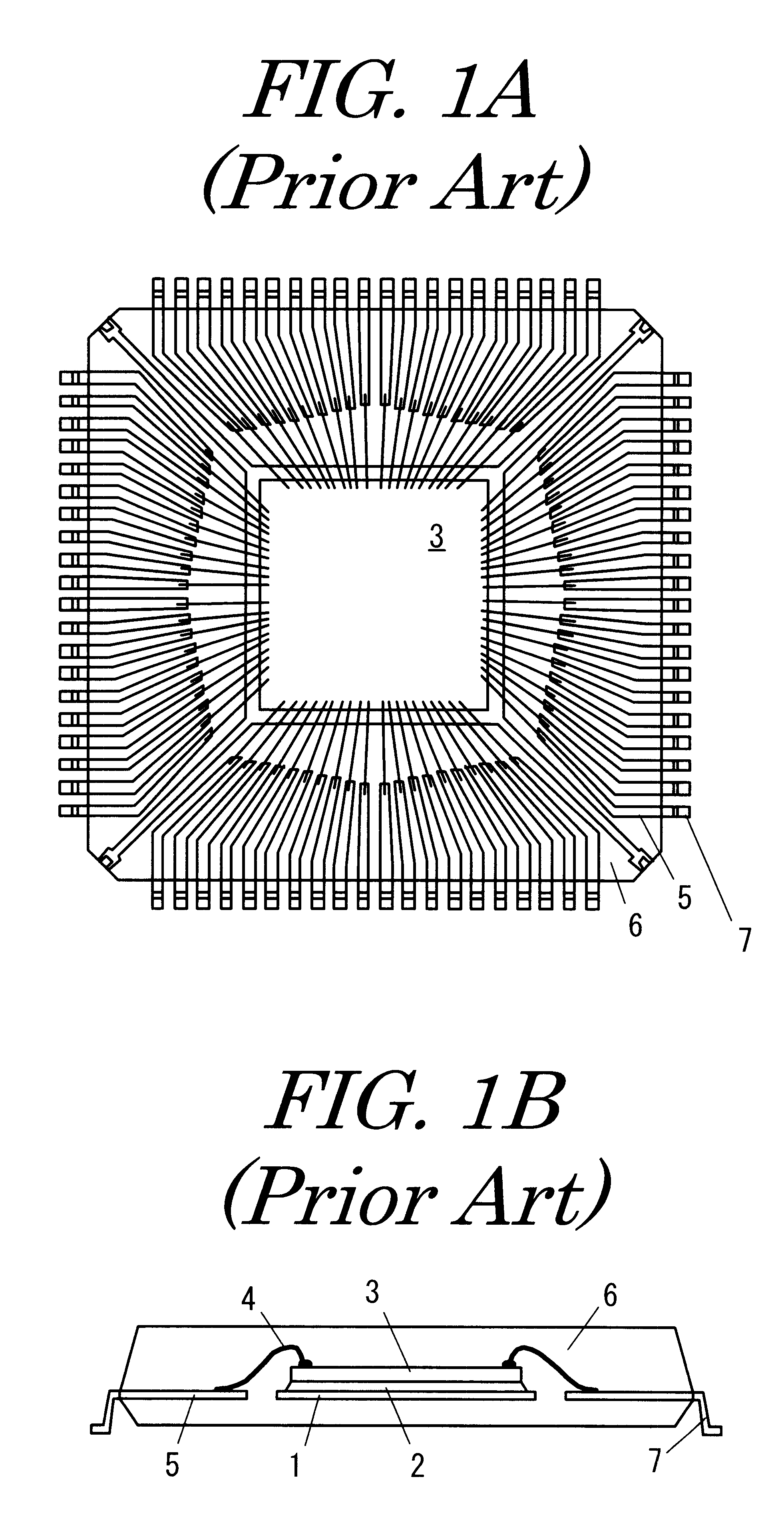
FIG. 3 is a plane view showing an inside of a lead frame type of semiconductor package according to a first preferred embodiment of the present invention. FIG. 4 is a cross-sectional view showing an inside of the semiconductor package, shown in FIG. 3. The semiconductor package according to the first preferred embodiment includes a die pad 101, a semiconductor device (chip) 103; inner leads 105 and a mold resin 106.

The semiconductor chip 103 is mounted on the die pad 101 using conductive paste 102. In the drawings, "P" represents a power supply terminal and "G" represents a ground terminal. The inner leads 105, connected to the power supply terminals P and ground terminals G, are extended inwardly toward the semiconductor chip 103. A chip capacitor mounting pad 111 is formed at the inner ends of the adjacent two extended inner leads 105. A chip capacitor 110 is mounted on each of the chip capacitor mounting pads 111 using conductive adhesives 112, such as silver-epoxy system adhesiv...

second preferred embodiment

FIG. 5 is a plane view showing an inside of a lead frame type of semiconductor package according to a second preferred embodiment of the present invention. FIG. 6A is a cross-sectional view showing a part of inner leads of the semiconductor package, shown in FIG. 5. FIG. 6B is a cross-sectional view taken on line A-A' of FIG. 6A. The semiconductor package according to the second preferred embodiment includes a semiconductor device (chip) 203, inner leads 205 and outer leads 207. In the drawings, "P" represents a power supply terminal and "G" represents a ground terminal.

In this embodiment, the power supply terminals P and ground terminals G are arranged adjacent or next to each other. High dielectric constant material 213 is arranged between adjacent power supply terminal P and ground terminal G so as to form a decoupling capacitor between those terminals. Surface electrodes on the semiconductor chip 203 are connected to the power supply terminals P, ground terminals G and signal te...

third preferred embodiment

FIG. 7 is a plane view showing an inside of a lead frame type of semiconductor package according to a third preferred embodiment of the present invention. FIG. 8A is a cross-sectional view showing an inside of the semiconductor package, shown in FIG. 7. FIG. 8B is a cross-sectional view showing an inside of the semiconductor package, shown in FIG. 7. The semiconductor package according to the third preferred embodiment includes a die pad 301, a semiconductor device (chip) 303 and inner leads 305. The semiconductor chip 303 is mounted on the die pad 301 using conductive paste 302. In the drawings, "P" represents a power supply terminal and "G" represents a ground terminal.

The die pad 301 is expanded outwardly to form a bonding area 314 for ground. Chip capacitors 310 are arranged between the bonding area 314 and the inner leads 305 for power supply terminals "P". Each of the chip capacitors 310 is connected to the inner leads 305 and bonding area 314 using conductive adhesives 312, s...


PUM


Abstract

A lead frame type of semiconductor apparatus includes a die pad on which a semiconductor chip is mounted; ground terminals which are to be grounded; power supply terminals which are connected to a power supply; inner leads connected to the ground terminals and power supply terminals, in which a pair of adjacent inner leads for power supply terminal and ground terminal are extended inwardly; a chip capacitor mounting pad which is provided at inner ends of the extended inner leads; and a chip capacitor which is mounted on the chip capacitor mounting pad so that a decoupling capacitor is provided.

Description

The present invention generally relates to a semiconductor apparatus having a decoupling capacitor.A conventional semiconductor chip is provided with electrodes connected to inner leads, arranged around a die pad. The die pad, semiconductor chip, bonding wires, and the inner leads are molded by a mold resin, such as an epoxy resin. The semiconductor package includes outer leads, which are extending outwardly from the package.A motherboard is provided at the inner layer and outer layer with copper wiring patterns. The motherboard is also provided at both upper and lower surfaces with terminals on which semiconductor devices and chips are mounted. A semiconductor device and chips, such as resistances and capacitors, are mounted on the motherboard using solder paste.The semiconductor package includes a chip capacitor used in order to reduce a power supply / ground noise. The chip capacitor is arranged between conductive patterns to which power supply terminal and ground terminal are conn...

Claims


Application Information

Patent Timeline
Patent Type & Authority Patents(United States)
IPC IPC(8): H01L23/58H01L23/48H01L23/64H01L23/495H05K1/02H05K1/18
CPCH01L23/49503H01L23/49589H01L23/50H01L23/642H01L24/32H01L24/48H01L24/49H01L23/3128H01L23/13H01L2924/07802H01L23/49816H01L23/49838H01L2224/05599H01L2224/27013H01L2224/32057H01L2224/32225H01L2224/32245H01L2224/48091H01L2224/48227H01L2224/48237H01L2224/48247H01L2224/48257H01L2224/48465H01L2224/4911H01L2224/49171H01L2224/73265H01L2224/83051H01L2224/83385H01L2224/85447H01L2924/01005H01L2924/01006H01L2924/01013H01L2924/01015H01L2924/01022H01L2924/01029H01L2924/01047H01L2924/01078H01L2924/01079H01L2924/01082H01L2924/014H01L2924/12044H01L2924/15153H01L2924/15165H01L2924/15173H01L2924/15311H01L2924/19041H01L2924/19103H01L2924/19105H01L2924/19106H01L2924/19107H01L2924/30107H05K1/0231H05K1/183H01L2924/00014H01L2924/01033H01L2224/26175H01L2224/291H01L2224/45099H01L2924/00H01L2924/00012H01L2224/32013H01L2924/00011H01L2924/181H01L24/73H01L2224/05647H01L2224/48H01L2224/49H01L2924/15158H01L2224/2612H01L2224/8384
Inventor TERUI, MAKOTOANZAI, NORITAKA
Owner LAPIS SEMICON CO LTD
Why Eureka
Try Eureka