Laser intrusive technique for locating specific integrated circuit current paths

a technology of integrated circuit current path and laser intrusion, which is applied in the direction of electronic circuit testing, measurement devices, instruments, etc., can solve the problems of parts that cannot pass the required tests or otherwise be deemed defective, parts that cannot be determined exactly what causes the defective part to fail the required tests, and parts that cannot be determined. , to achieve the effect of reducing noise, reducing the noise floor, and being more sensitive to voltage alterations

Inactive Publication Date: 2003-09-09
GLOBALFOUNDRIES INC
View PDF8 Cites 113 Cited by
  • Summary
  • Abstract
  • Description
  • Claims
  • Application Information

AI Technical Summary

Benefits of technology

The present invention is expected to alleviate the problems described above because the global power supply provides the quiescent current to the IC. The separate dedicated power supply then has a lower noise floor and is more sensitive to voltage alterations, especially from marginally defective devices. Therefore, a voltage alteration on the dedicated power supply is measured independent of any background noise resulting from the quiescent state of the IC. Also, if the dedicated power supply supplies power only the suspect area of the IC, then a greater sensitivity is achieved when the laser is scanned over that area. This same premise is expected to provide promising results even as new generations of ICs are developed which require more current.

Problems solved by technology

Some parts may not pass the required tests or may otherwise be deemed defective.
For example, if an input / output pin on the IC has a current leakage path it may be deemed defective.
Many times in developing and manufacturing ICs it is difficult to determine exactly what causes the defective part to fail the required tests.
IC technology trends only exacerbate this problem as more routing layers are required to connect tightly packed circuit elements.
In addition, the number of transistors in each successive generation of ICs are doubling approximately every eighteen months, which results in a continual increase in total current demand with each new generation of ICs.
These local current changes alter the total power required, and these changes are more pronounced when the light source is exposed to a defect on the IC.
Therefore a voltage alteration on the power supply caused by light exposure may indicate that a defect in the area of the IC that is being exposed to the light source.
However, these methods have weaknesses that cause defects to be overlooked.
Another problem is that circuit elements that are only marginally defective may not produce enough of a current change when exposed to the light source to overcome the noise floor and be noticed.
With millions of circuit elements (specifically transistors) in a typical IC, the overall noise floor can be quite high.
In such circumstances, a marginally defective transistor that produces less of a current change than a fully defective transistor with respect to the overall quiescent current draw is more likely to remain unnoticed.
In addition, because current demands (both quiescent and dynamic) in successive generations of ICs increase every eighteen months, the current risk becoming less and less capable of detecting defects.

Method used


Image

  • Laser intrusive technique for locating specific integrated circuit current paths
  • Laser intrusive technique for locating specific integrated circuit current paths
  • Laser intrusive technique for locating specific integrated circuit current paths

Examples


Embodiment Construction

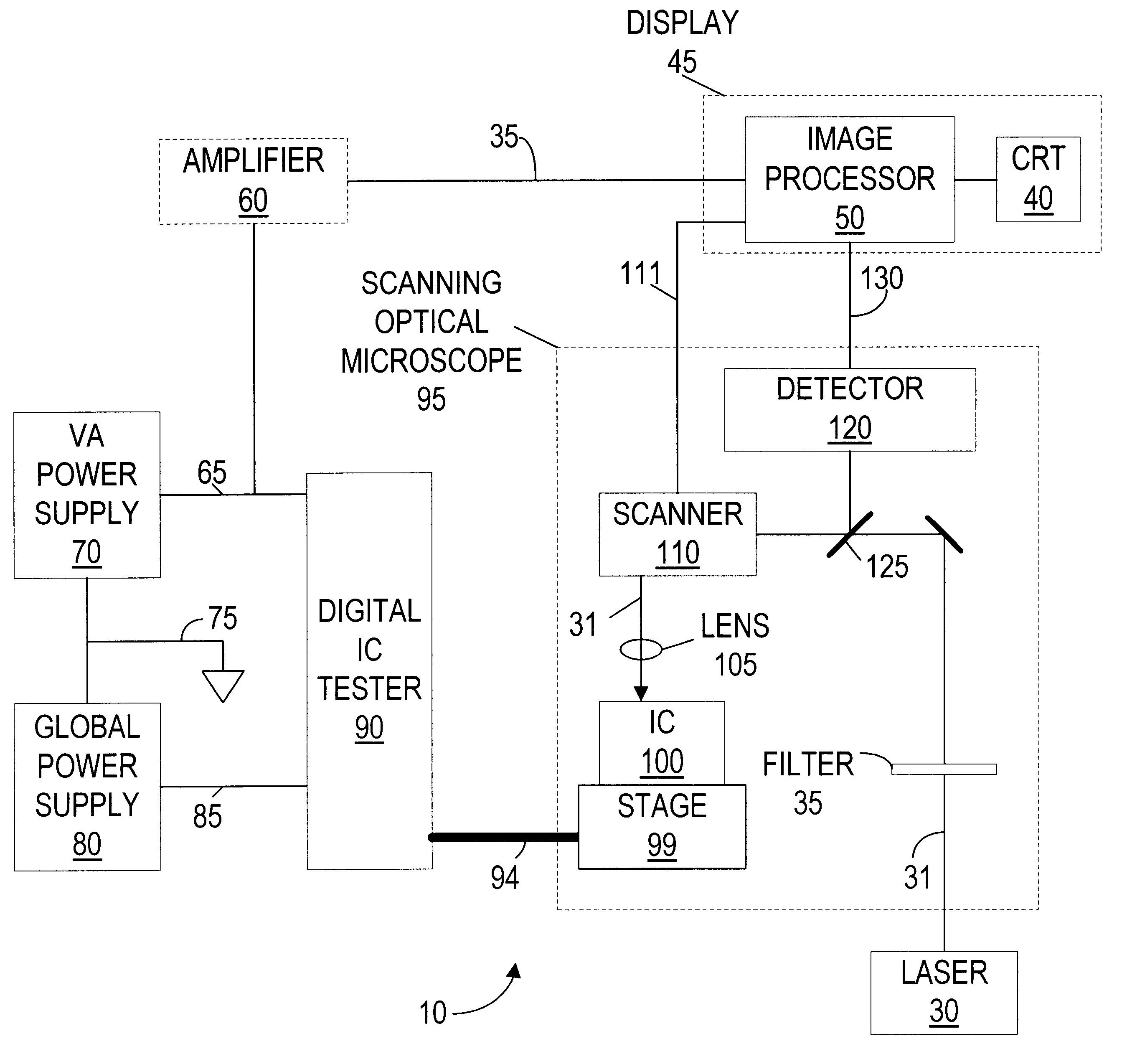
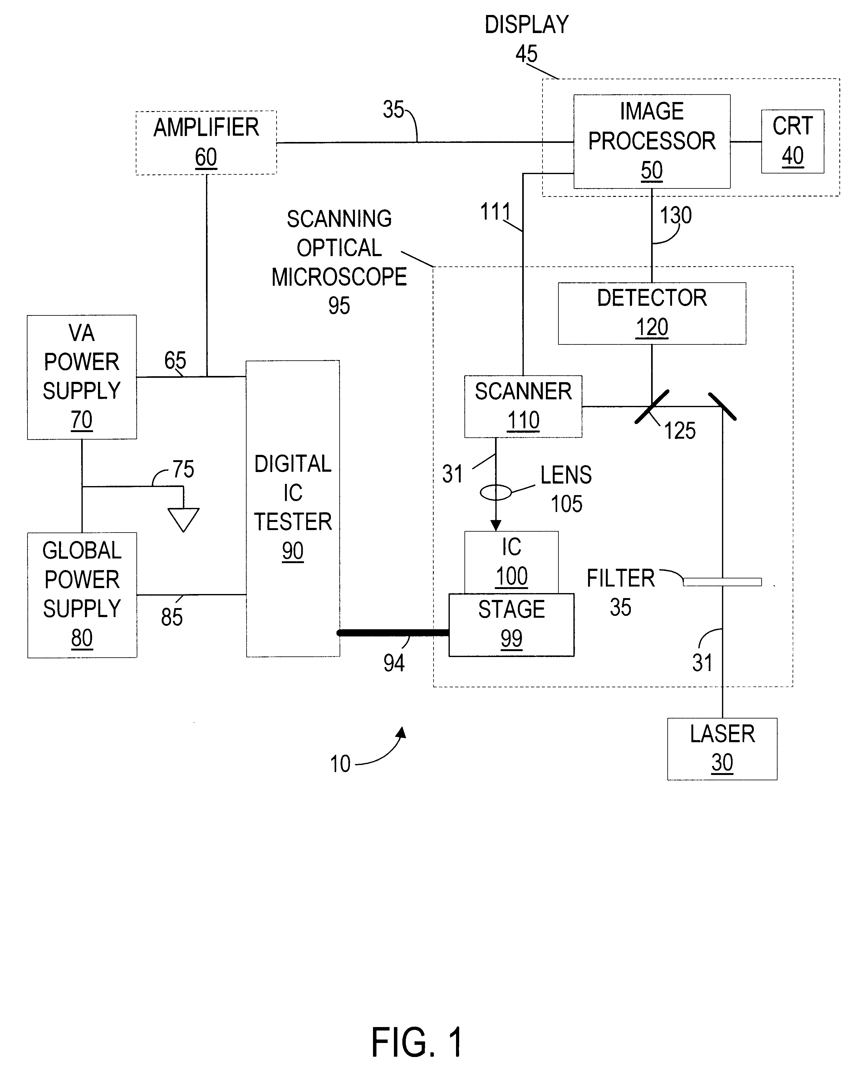
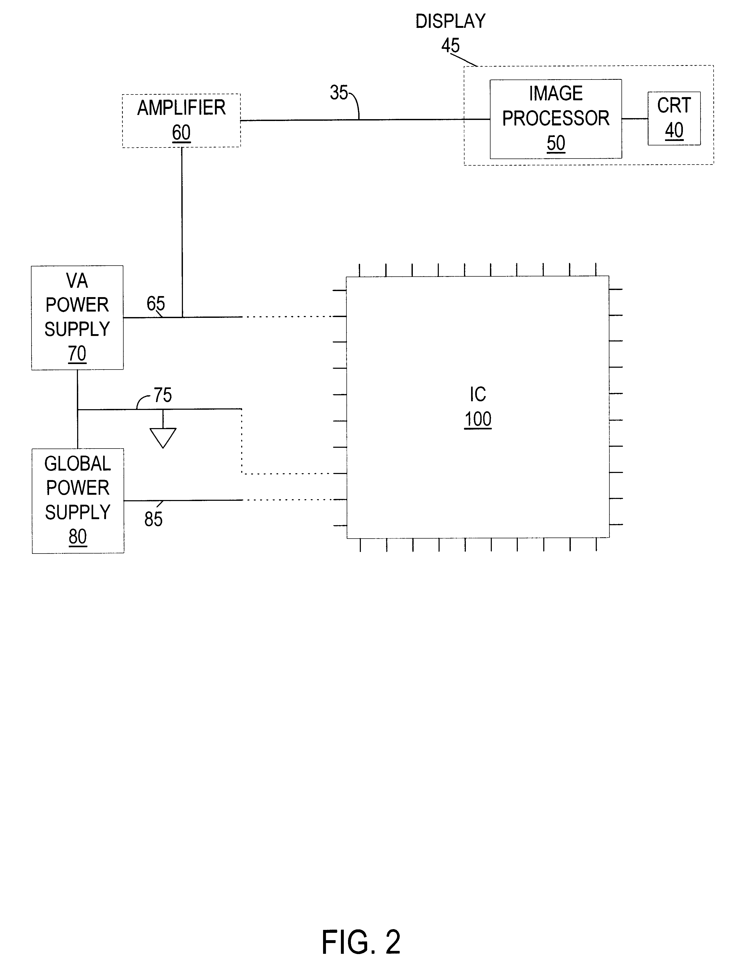
The present invention provides an improved defect detection technique and system. In a preferred embodiment, the defect detection system includes two separate power supplies: a global power supply and a dedicated power supply. The global power supply provides power to the IC and is preferably a constant voltage power supply. The dedicated power supply supplies power to specific points of interest on the IC, and may be a variable current and / or a variable voltage power supply. The dedicated power supply may be configured to supply a constant current approximately equal to a previously measured value while letting the voltage vary. Next the IC is scanned with the light source, and the defect causes a change in power demand on the dedicated power supply when exposed to the light source. This change in power demand is the result of photon exposure or localized heating of the IC, and is more of a drastic change when the light is exposed to a defect on the IC. The change in power demand c...


PUM


Abstract

A method and apparatus for locating integrated circuit defects associated with different aspects of the integrated circuit industry. The integrated circuit is configured in a known failing mode, with a first power supply providing a constant voltage and variable current. Next, one or more additional dedicated power supplies are connected to various points of interest throughout the integrated circuit, wherein these dedicated power supplies have a preset current and the voltage is allowed to vary. The integrated circuit is then scanned with a laser beam, which induces current changes on in the integrated circuit especially in defective areas. These current changes then cause voltage changes on the dedicated power supplies. When such a voltage change occurs on the dedicated power supplies, its position is noted.

Description

1. Field of the InventionThe present invention relates generally to failure analysis and device qualification in integrated circuits, as well as design debugging. More particularly, the present invention relates to an improved method of locating specific integrated circuit current paths that are related to defects, mis-processing or poor circuit design.2. Description of Related ArtIn integrated circuit ("IC") manufacturing, parts are tested throughout various stages of fabrication and packaging. Some parts may not pass the required tests or may otherwise be deemed defective. For example, if an input / output pin on the IC has a current leakage path it may be deemed defective. Many times in developing and manufacturing ICs it is difficult to determine exactly what causes the defective part to fail the required tests. IC technology trends only exacerbate this problem as more routing layers are required to connect tightly packed circuit elements. In addition, the number of transistors in...

Claims


Application Information

Patent Timeline
Patent Type & Authority Patents(United States)
IPC IPC(8): G01R31/28G01R31/311G01R31/319
CPCG01R31/311G01R31/31905
Inventor BRUCE, VICTORIA J.
Owner GLOBALFOUNDRIES INC
Why Eureka
Try Eureka