Photonic bandgap device using coupled defects

a bandgap device and coupled defect technology, applied in the direction of optical waveguide light guide, instruments, nanotechnology, etc., can solve the problems of discontinuous defect photonic bandgap, coupling and fragility problems, and serious device integration,

Inactive Publication Date: 2003-09-09
RPX CLEARINGHOUSE
View PDF8 Cites 66 Cited by
  • Summary
  • Abstract
  • Description
  • Claims
  • Application Information

AI Technical Summary

Problems solved by technology

It is caused by interference effects arising from periodicity in the structure of the material.
Such devices also have light containment problems in the third or vertical direction and serious device integration, coupling and fragility problems.
However

Method used


Image

  • Photonic bandgap device using coupled defects
  • Photonic bandgap device using coupled defects
  • Photonic bandgap device using coupled defects

Examples


Embodiment Construction

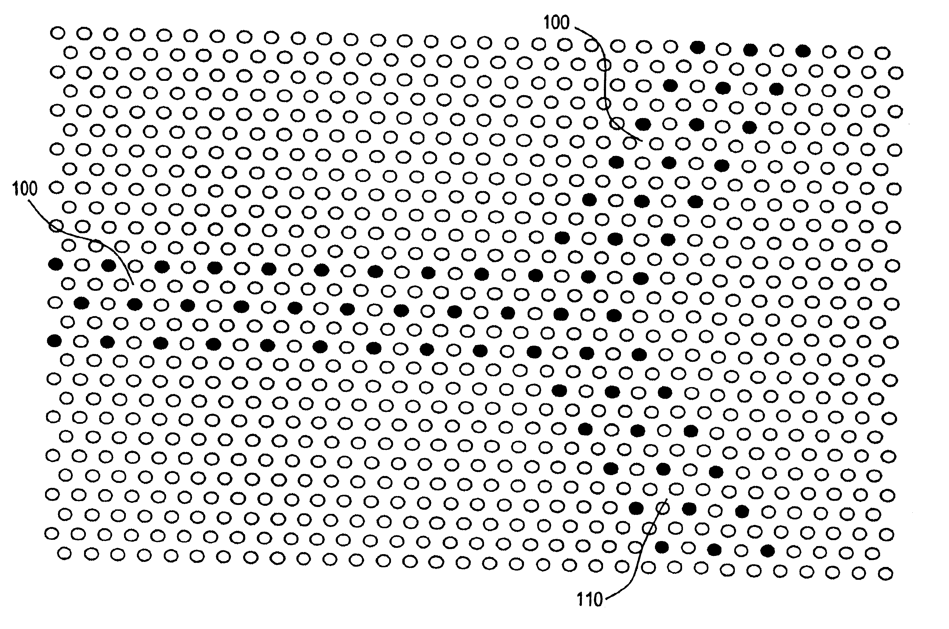
By way of introduction to the examples of how to implement the above mentioned features, first, transmission response of a photonic crystal having a hexagonal lattice structure, with and without a mesh of defects, will be described. Then, various different meshes will be explained, before describing waveguide configurations and applications, using the meshes or lines of defects.

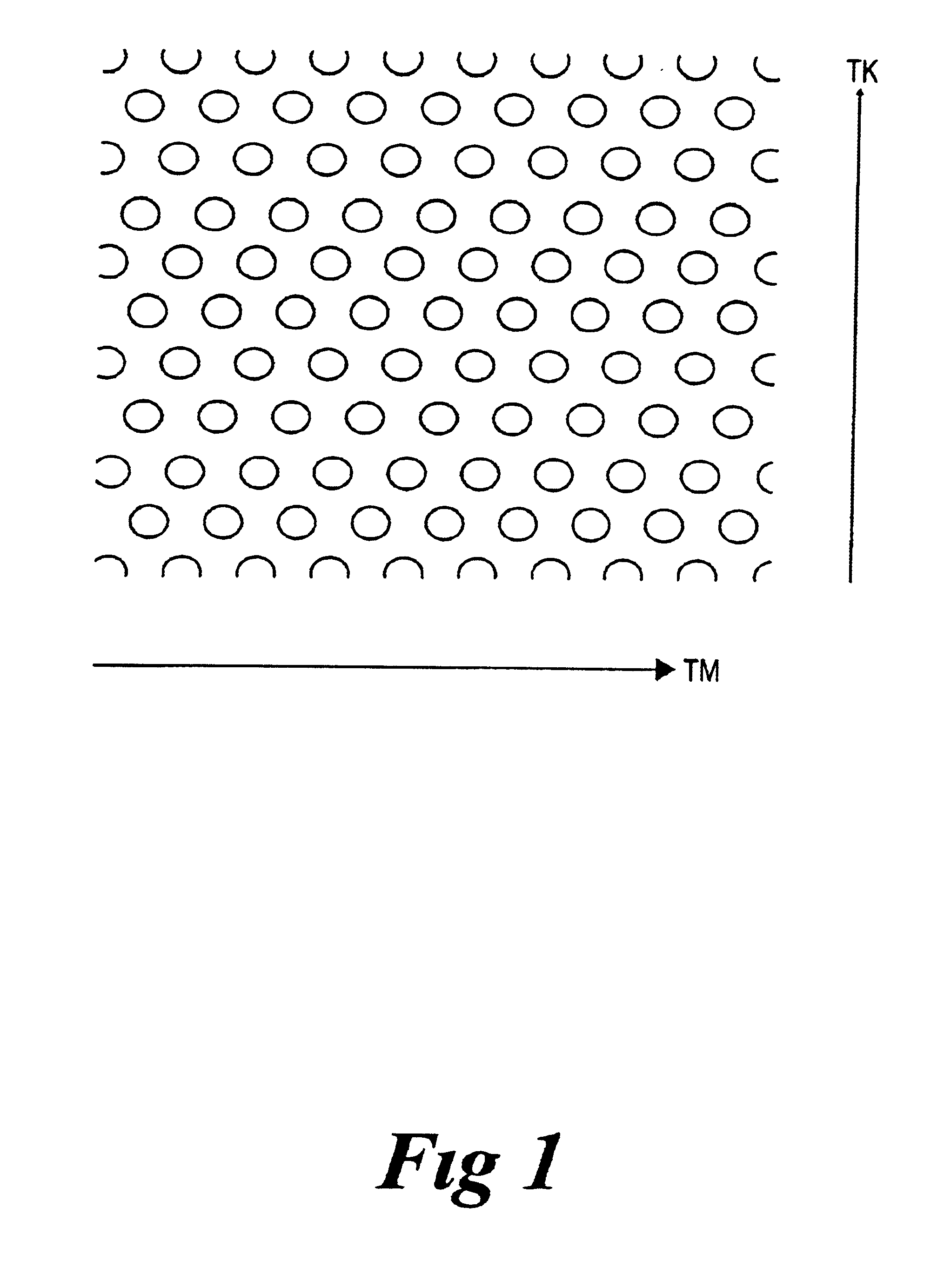
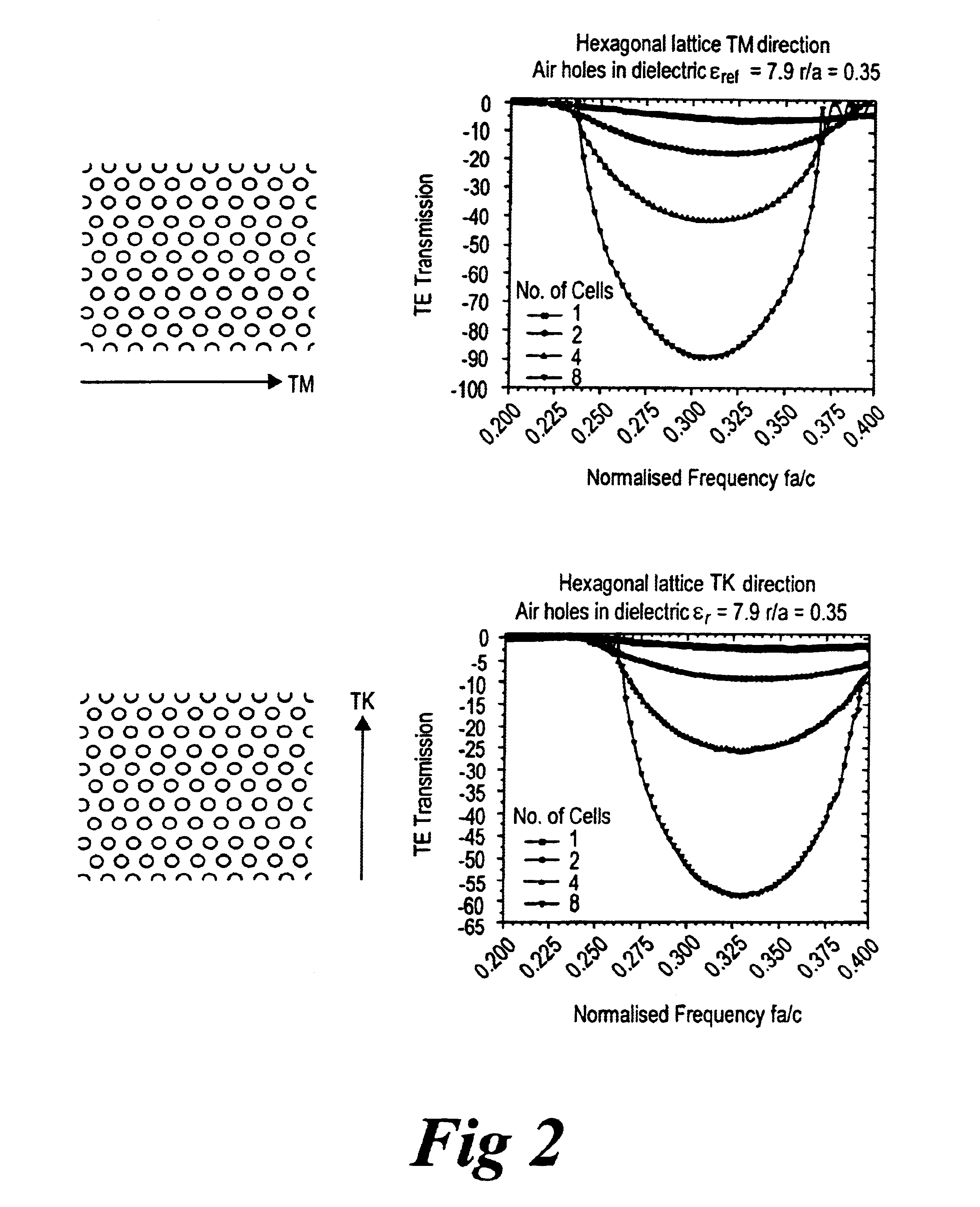
FIGS, 1 and 2, Perfect Crystal Before Defects are Introduced

A section of a hexagonal lattice before defects are introduced is shown in FIG. 1 and the two main crystal directions are labelled within the figure, .GAMMA.M and .GAMMA.K. The refractive index of the material was chosen to be nmaterial=2.81 resulting in a dielectric constant of er=7.9. These figures are representative of the effective index of a GaAs waveguide that is 1 / 2 mm thick, with oxidised AlGaAs on one side, nAIOx=1.6, and air on the other for application at 1.5 mm. The air cylinders in the material were chosen to have a ratio of radius, r, t...


PUM


Abstract

A photonic bandgap device has a lattice structure, with a waveguide formed by a mesh of defects in the lattice, the defects being located discontinuously, but sufficiently close to each other to provide coupling between overlapping evanescent defect modes. By changing shape and configuration of the mesh and varying the types of defects, it is easier to control the width and position of the transmission band, in wavelength terms, compared to a waveguide formed only from a planar defect, i.e. a single line of defects. Multiplexers, demultiplexers, filters, switches, combiners, and splitters may be created. Many devices and different types of devices can be integrated onto the same crystal lattice, with far greater compactness than planar waveguide technology. The mesh can have a periodic structure of lines of defects, or periodic spacing between defects to reduce loss.

Description

The invention relates to photonic band gap devices having waveguides, to optical wavelength demultiplexers, optical filters, and optical switches, particularly for use in optical communications. It also relates to integrated optical circuits, nodes for an optical network, methods of transmitting data using integrated optical circuits, and to software arranged to control the integrated optical circuits, again particularly for use in optical communications.BACKGROUND TO THE INVENTIONOptical or microwave components making use of the concept of a photonic bandgap (PBG) are known. The definition of a photonic bandgap material is commonly accepted as being a material having a property that electromagnetic radiation, (such as light) of a range of wavelengths, is not permitted to exist when the light is incident on a given part of the material at a range of angles. This can be seen as a dip or gap in the wavelength response, hence the name "bandgap". It is caused by interference effects ari...

Claims


Application Information

Patent Timeline
IPC IPC(8): G02B6/122G02B6/12
CPCB82Y20/00G02B6/12007G02B6/1225
Inventor REYNOLDS, ANDREW L
Owner RPX CLEARINGHOUSE
Why Eureka
Try Eureka