Package socket and package legs structure for led and manufacturing of the same

a technology of led and packaging sockets, which is applied in the direction of discharge tubes, luminescnet screens, instruments, etc., can solve the problems of insufficient focus of ellipsoid, difficult manufacturing, and difficult production of tools, so as to reduce the width of the package, less pc board area, and easy hole drilling of the pc board

Inactive Publication Date: 2003-09-16
HEN CHANG HSIU
View PDF7 Cites 41 Cited by
  • Summary
  • Abstract
  • Description
  • Claims
  • Application Information

AI Technical Summary

Benefits of technology

is to provide an LED packaging socket and package legs structure which can decrease the width of the package such that less PC board area is needed, hole drilling of the pc board is more easily and plating in the hole is more uniform, which gives a better contact, these make the manufacturing of LED array more easily.
Another object of the present invention is to provide an overlap cascaded packaging structure of a full color semiconductor LED with reflected metal layer to enhance the intensity of light.
Another object of the present invention is to provide an LED package socket and package legs structure that the LED package is round shape, the round-shape parabola side-wall of the socket reflect and focus the light then emit forward to increase the intensity, the surface of the transparent epoxy seal also form round-shape focus lens which will give better focus and imaging effect.
The other object of the present invention is to provide an LED package socket and package legs structure, which can be used in an multi-color overlap cascaded LED packaging, the length of the bonding wire can be decreased, so that reliability can be increased and wire resistant can be reduced.
The other object of the present invention is to provide a manufacturing method of LED package socket and package legs structure, wherein the four package legs can be stand along on the corner of a square and surface mount is possible, assembling is more easily and need not to drill holes in the PC board.
The other object of the present invention is to provide a manufacturing method of LED package socket and package legs structure, so that punching is operated in the same direction to decrease the difficulty of punch operation.

Problems solved by technology

For smaller package, the space must be deceased so that the tooling is difficult to produce, and manufacturing is also difficult.
The focus of the ellipsoid is not good enough.
However, This LED die can not use the traditional three-leg package structure.
Using four-leg package structure will increase the width of the package, if decrease the width by decreasing the width and space between package legs will make the hole drilling on the PC board more difficult, and smaller hole diameter will make electrode plating not uniform.

Method used


Image

  • Package socket and package legs structure for led and manufacturing of the same
  • Package socket and package legs structure for led and manufacturing of the same
  • Package socket and package legs structure for led and manufacturing of the same

Examples


second embodiment

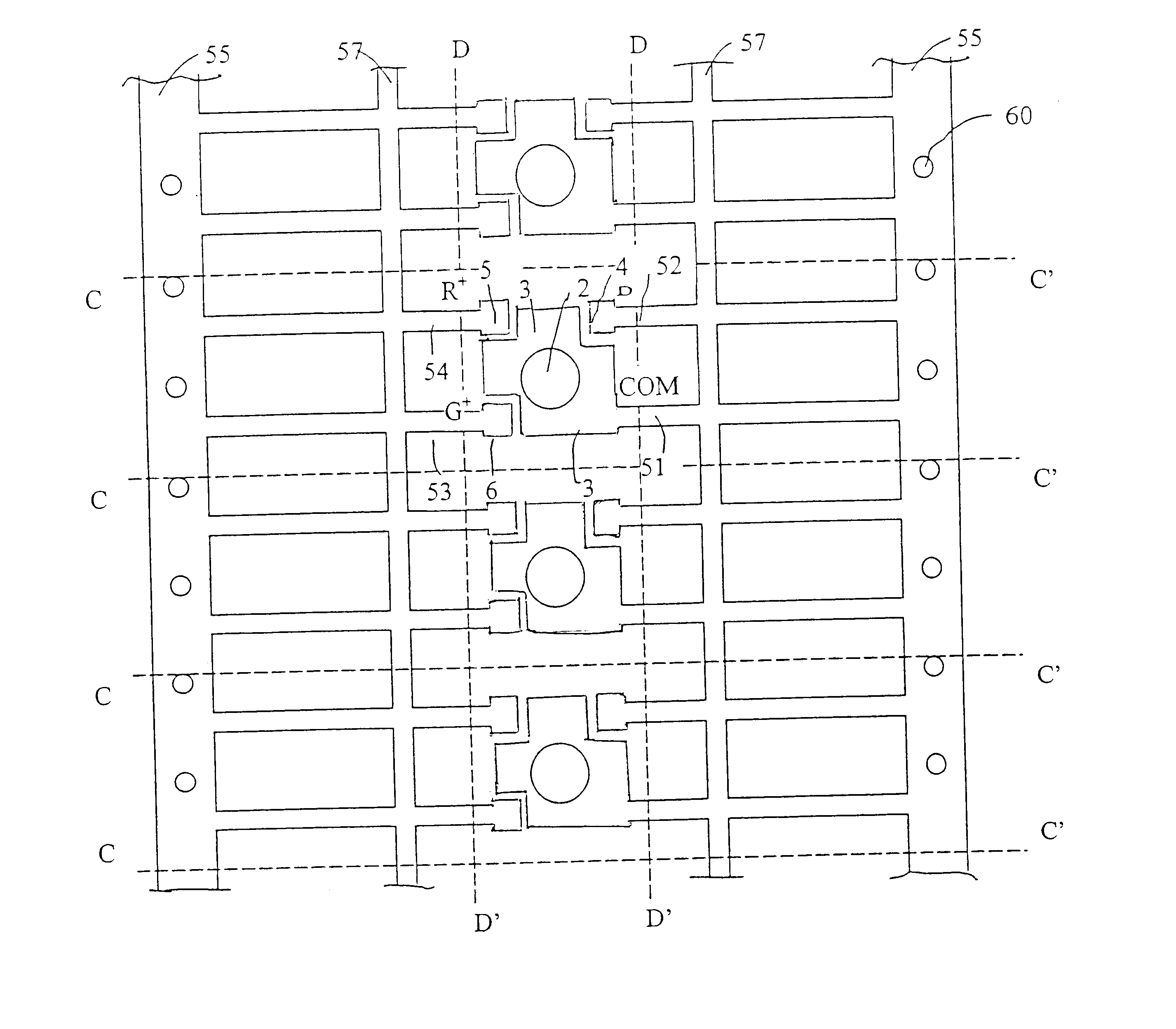
According to the present invention, after punched a metal plate and form the structure as shown in FIG. 5, die-bond and wire-bond are performed first and then bend the legs 90.degree. along line D-D', then completed sealing with transparent epoxy (not shown) and cut away the small tie bars 57 and large tie bars 55, so automatic manufacturing can be used for mass production. This is one of the advantages of the present invention.

third embodiment

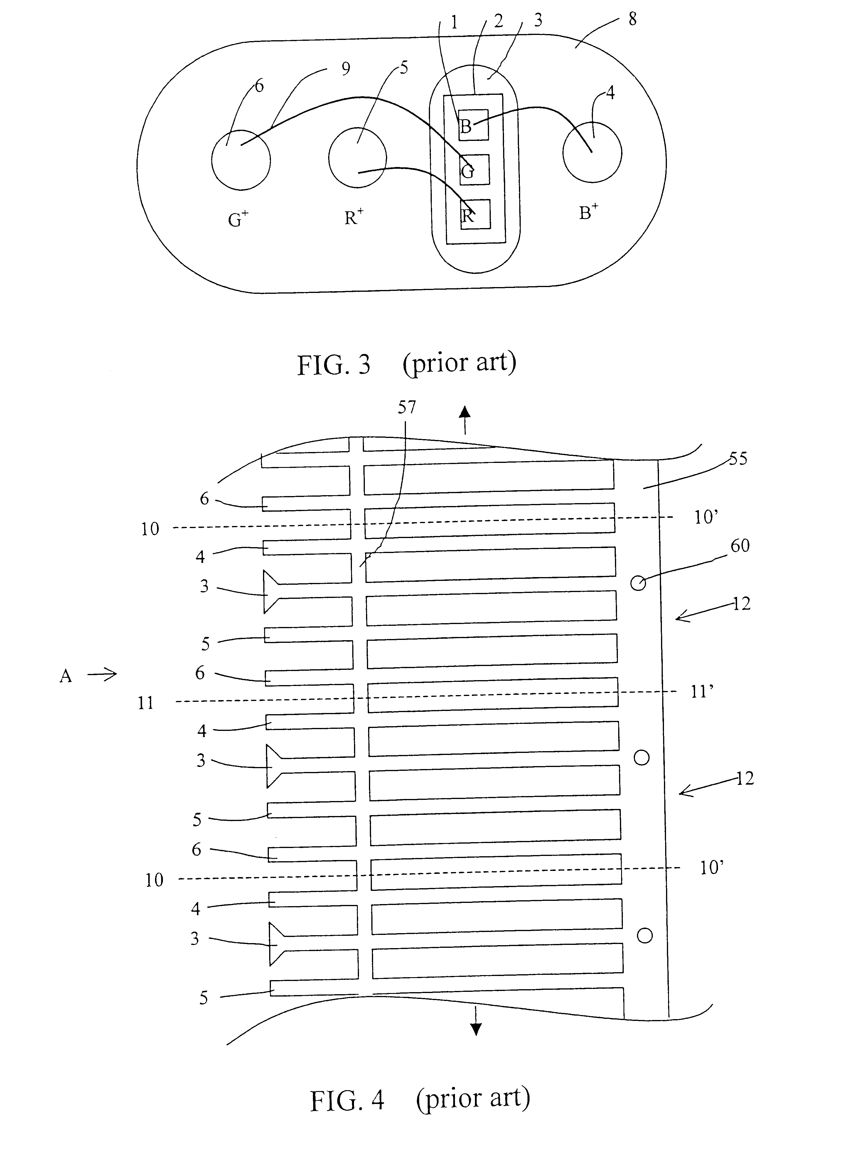
According to the present invention, as shown in FIG. 10, after completed sealing with transparent epoxy 8 and cut away the small tie bars 57 and large tie bars 55, by bending the end of the four legs inward or outward so that the package can be used in surface mount technology on a PC board, the PC board need not drilling holes and plating in the holes to eliminate packaging steps, and is more easy to make LED array on a PC board. This is one of the advantages of the present invention.


PUM


Abstract

The present invention discloses a structure of package socket and package legs for three-primary-color LED and the manufacturing method of this structure. One of the leg forms a die bonding seat and a common negative bonding pad, the other three legs form positive bonding pads. Said negative and positive bonding pads are arranged in the four corners of a square, with two legs stretch to the right, the other two legs stretch to the left. Then punch by a punch machine with a tooling to form an array of the structures, or by electrode plating or by etching to form the array. The four legs are then bending 90° to one side near the bonding pads such that it can stand alone. After die bond and wire bond has performed, the LED is sealed by transparent epoxy molding, and then cut to single structures, or the structure is cut to single structures before the LED is sealed by transparent epoxy. The other structure is by further bending the four legs near the end of the legs to satisfy surface mount technology (SMT).

Description

1. Field of the InventionThe present invention related to light emitting diode (LED) packaging technology more particularly, to a package socket and package legs structure and manufacturing method for three-primary-color LED packaging.2. Description of Relative Prior ArtThe conventional mono-color LED package structure has two package legs, two-color LED has three package legs, and three-primary-color (red, blue and green) LED may have three or four package legs. FIG. 1 shows the cross sectional view of the package structure of a mono-color LED with two package legs. One of the package leg form the negative bond pad 3 has a socket to form a die seat 2, LED die 1 is die bonded on the die seat 2, the other package legs form the positive bond pad 4, the positive and negative electrode of the die is then wire bond to the positive and negative bond pad, respectively. Finally seal with transparent epoxy 8, which also form a round-shape focus lens. FIG. 2 shows the cross sectional view of ...

Claims


Application Information

Patent Timeline
Patent Type & Authority Patents(United States)
IPC IPC(8): H01L33/00H01J13/46H01J1/00H01K1/00H01J13/00H01K1/62H01J1/62H01L27/14H01L25/075H01L33/62
CPCH01L25/0753H01L33/62Y10S362/80H01L2224/48091H01L2224/48247H01L2224/73265H01L2924/00014H01L2224/32245H01L2924/00H01L2224/32257H01L2224/48257
Inventor HEN, CHANG HSIU
Owner HEN CHANG HSIU
Why Eureka
Try Eureka