Alternating current driven type plasma display
a technology of alternating current and plasma display, which is applied in the direction of gas discharge electrodes, sustain/scan electrodes, gas-filled discharge tubes, etc., can solve the problems of deteriorating durability, reliability and lifetime, affecting the quality of display, and reducing the extent of abnormal discharge, so as to prevent the occurrence of abnormal discharge. , the effect of reducing the size of the portion where abnormal discharge has taken pla
- Summary
- Abstract
- Description
- Claims
- Application Information
AI Technical Summary
Benefits of technology
Problems solved by technology
Method used
Image
Examples
example 1
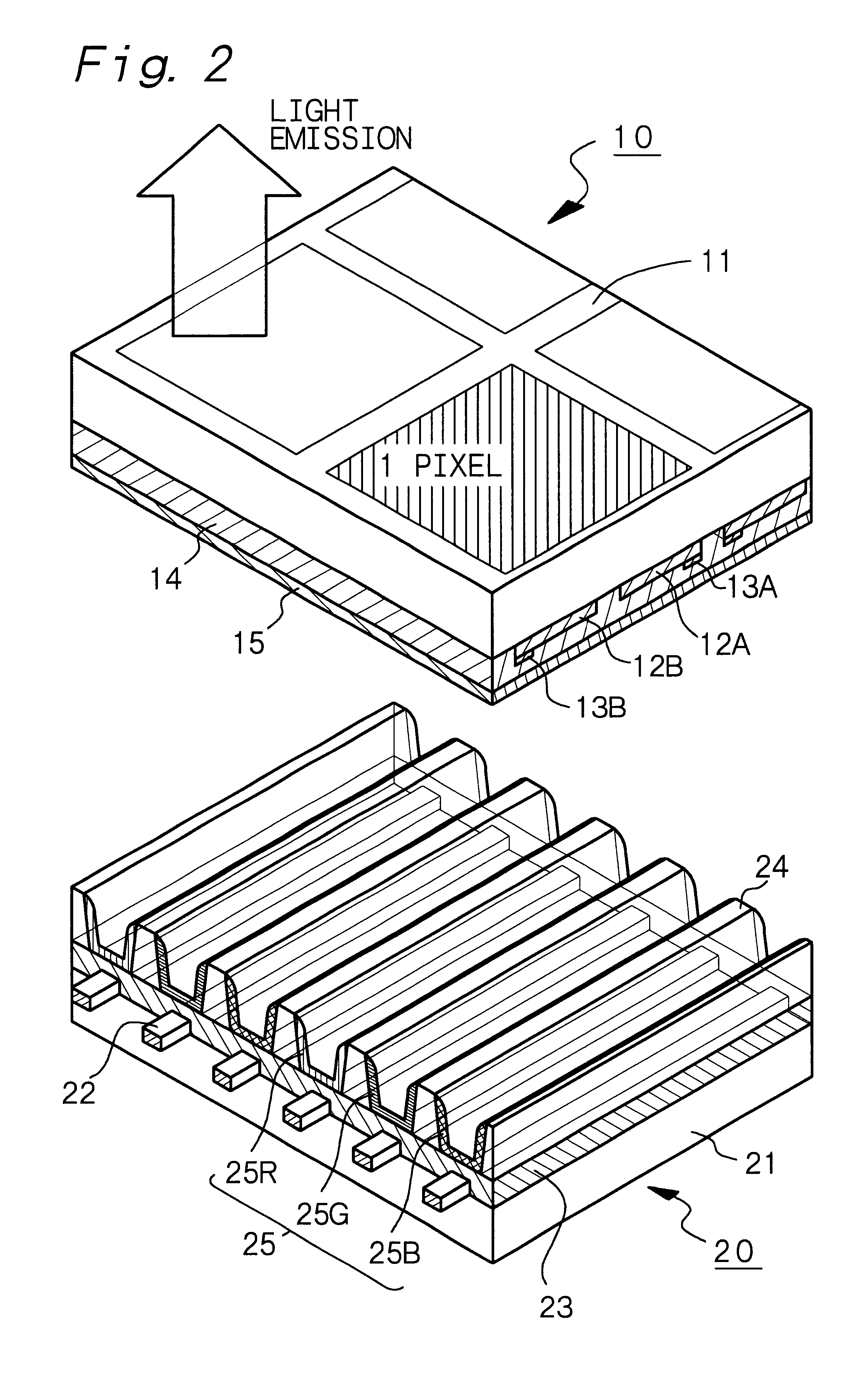
is concerned with a plasma display according to the first aspect of the present invention. As shown in the schematic exploded perspective view of FIG. 2, the plasma display comprises a first panel 10 (corresponding to a front panel) and a second panel 20 (corresponding to a rear panel). The first panel 10 has electrode groups formed on a transparent first substrate 11 made, for example, of glass and a dielectric layer 14 made of a glass paste and formed on the first substrate and also on the electrode groups. These first panel 10 and the second panel 20 are bonded to each other in their circumferential portions. Further, a protective layer 15 made of MgO is formed on the dielectric layer 14.
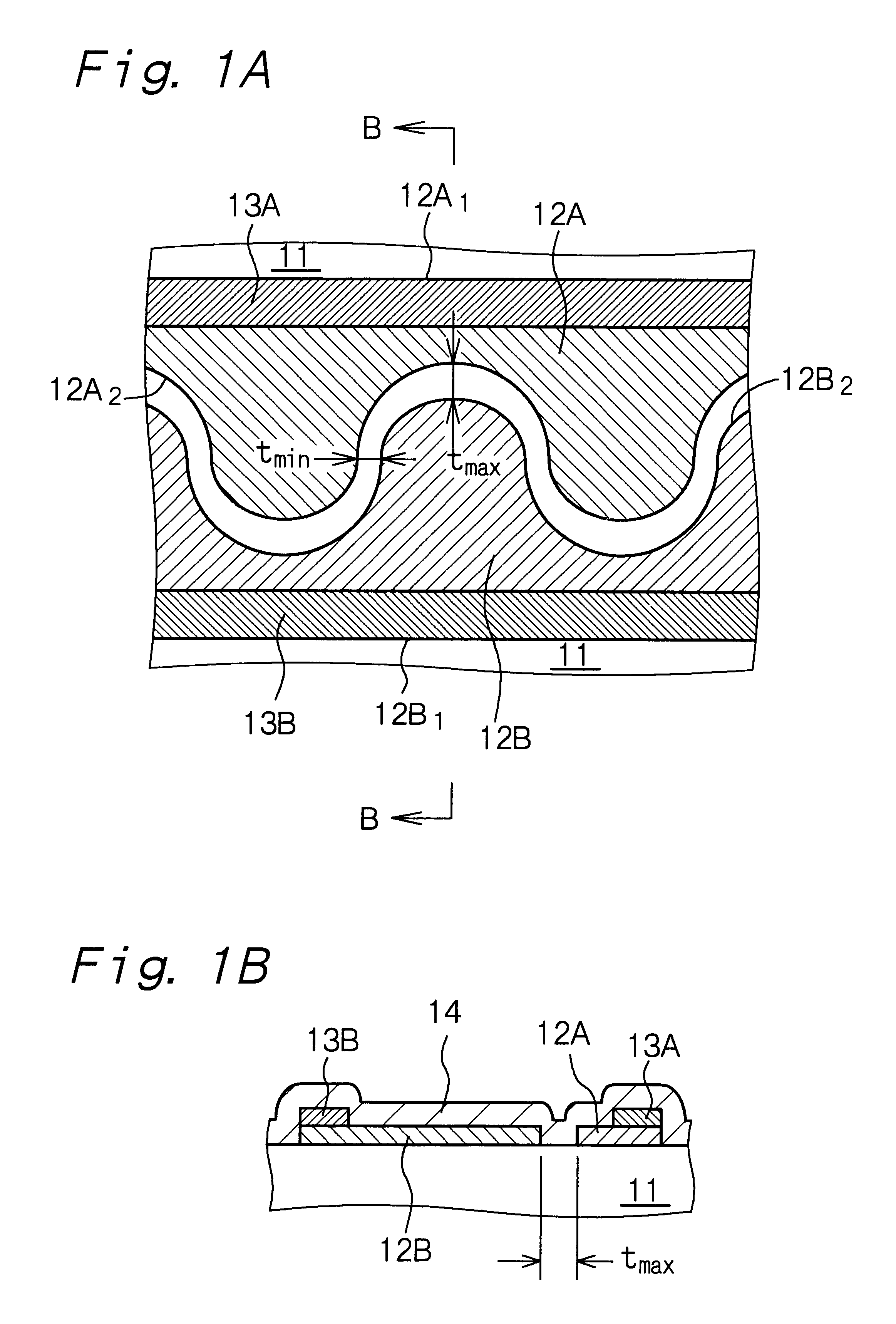
FIG. 1A shows a schematic layout of the electrode group, and FIG. 1B shows a schematic partial cross-sectional view of the first panel 10 taken along arrows B--B in FIG. 1A. For clarifying the electrodes in FIG. 1A, the electrodes are provided with slanting lines. In FIG. 1A, showing of the diele...
example 2
Example 2 is concerned with the plasma display according to the second aspect of the present invention. Since the basis structure of the plasma display of Example 2 is the same as that of the plasma display of Example 1, a detailed explanation thereof is omitted. Each of FIGS. 4A and 4B shows a schematic layout of the electrode group of the plasma display of Example 2. In FIGS. 4A and 4B, the electrodes are provided with slanting lines for clearly showing them. The dielectric layer 14 and the protective layer 15 are omitted from showing in these Figures.
Each electrode group of the plasma display of Example 2 comprises (A) a first bus electrode 13A, (B) a second bus electrode 13B extending in parallel with the first bus electrode 13A, (C) a first sustain electrode 112A having a projection portion 112a extending from the first bus electrode 13A toward the second bus electrode 13B, and (D) a second sustain electrode 112B having a projection portion 112b extending from the second bus el...
example 3
Example 3 is concerned with the plasma display according to the third aspect of the present invention. Since the basis structure of the plasma display of Example 3 is also the same as that of the plasma display of Example 1, a detailed explanation thereof is omitted.
Each of FIGS. 5A, 5B and 6 shows a schematic layout of the electrode group of the plasma display of Example 3. In FIGS. 5A, 5B and 6, the electrodes are provided with slanting lines for clearly showing them. The dielectric layer 14 and the protective layer 15 are omitted from showing in these Figures.
Each of the electrode groups of the plasma display of Example 3 comprises (A) a first bus electrode 13A, (B) a second bus electrode 13B extending in parallel with the first bus electrode 13A, (C) a first sustain electrode 212A having a projection portion 212a extending from the first bus electrode 13A toward the second bus electrode 13B, and (D) a second sustain electrode 212B having a projection portion 212b extending from ...
PUM
 Abstract
Description
Claims
Application Information


