Method for producing layered structures on a substrate, substrate and semiconductor components produced according to said method

a technology of layered structure and substrate, which is applied in the direction of sustainable manufacturing/processing, crystal growth process, final product manufacturing, etc., can solve the problems of increasing the danger of undesired separation, the method is relatively complicated, and the method is more complicated

Inactive Publication Date: 2003-11-11
MAX PLANCK GESELLSCHAFT ZUR FOERDERUNG DER WISSENSCHAFTEN EV
View PDF26 Cites 126 Cited by
  • Summary
  • Abstract
  • Description
  • Claims
  • Application Information

AI Technical Summary

Benefits of technology

It is also an object of the present invention to propose methods for the production of different novel substrates which form the starting point for the production of further structures by means of epitaxial methods. Moreover, it is an object of the present invention to provide a photocell and other semiconductor components using the method of the invention which can be manufactured at favorable cost and which have excellent technical characteristics.
Particularly important are the savings of time, effort and material which can be achieved by the use of structured layers, and indeed in particular when the structuring is exploited in the final product. Since the porous layer has a corresponding surface structuring, the layer-like structure can be provided with the same structuring.
That is to say, using the method of the invention, the porous layer can be made relatively thin, preferably in the range of about 100 nm to 10.mu., so that relatively little material is lost and the working speed is improved, particularly since the once produced surface structuring of the substrate can be exploited for the manufacture of a plurality of identically structured layer-like structures.
This type of separation of the layer-like structure from the substrate also succeeds when the surface of the porous layer is made flat. It is particularly favorable, in particular for the manufacture of the photocells or various other components, when the surface of the porous layer remote from the substrate is structured, since, on growing the layer-like structure on the porous layer, the layer-like structure reflects the structuring of the porous layer, so that, for example with a solar cell, the trapping of light takes place with substantially higher efficiency.
Since the structured surface of the substrate is preserved and can be reused, optionally after a cleaning step or after freshening up the structuring, a plurality of identical, layer-like structures can be manufactured from one substrate, which substantially increases the economy of the method, particularly since it is not necessary to newly structure the substrate every time.
Since the sections of the porous material layer remain bonded to each second substrate, any desired layer-like structures can be grown onto these substrates by means of the epitaxial methods. Since the alignment of the crystal structure in each section of the porous material layer is the same, the structures grown on the second substrates by epitaxial methods likewise have a monocrystalline structure, so that one can, starting from an expensive substrate, produce a plurality of substrates for epitaxial methods in a favorably priced manner.

Problems solved by technology

The method is, however, relatively complicated because the porous silicon layer must be etched away.
Even if the method step of the separation can be improved hereby, the method is more complicated and an increased danger exists of undesired separation prior to or during the production of the layer-like structure.
A multiple use of the starting substrate is admittedly achieved here; nevertheless one would, in many potential uses, use the expensive monocrystalline substrate in a relatively wasteful manner.
So far as is known, there are no methods which satisfy all these criteria.
If one, however, operates in accordance with the prior art, which aims at planar surfaces, it is first necessary to produce thicker layers which must then be structured in a complicated manner by the removal of material.
For this, the porous layer is first removed, since it is as a rule damaged.
This is not possible in the prior art, when the porous layer is removed by etching or by mechanical removal from the layer-like structure.

Method used


Image

  • Method for producing layered structures on a substrate, substrate and semiconductor components produced according to said method
  • Method for producing layered structures on a substrate, substrate and semiconductor components produced according to said method
  • Method for producing layered structures on a substrate, substrate and semiconductor components produced according to said method

Examples


Embodiment Construction

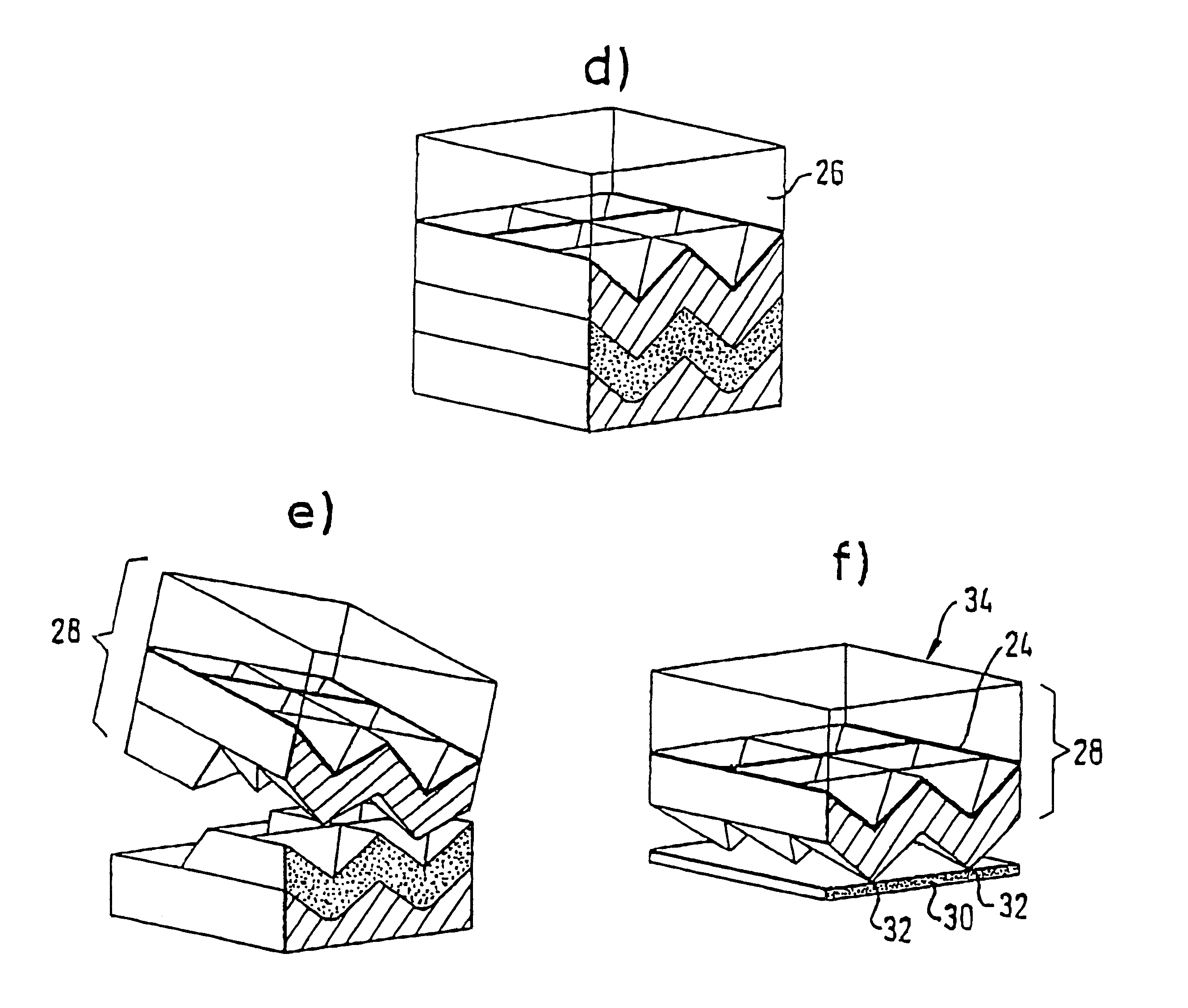
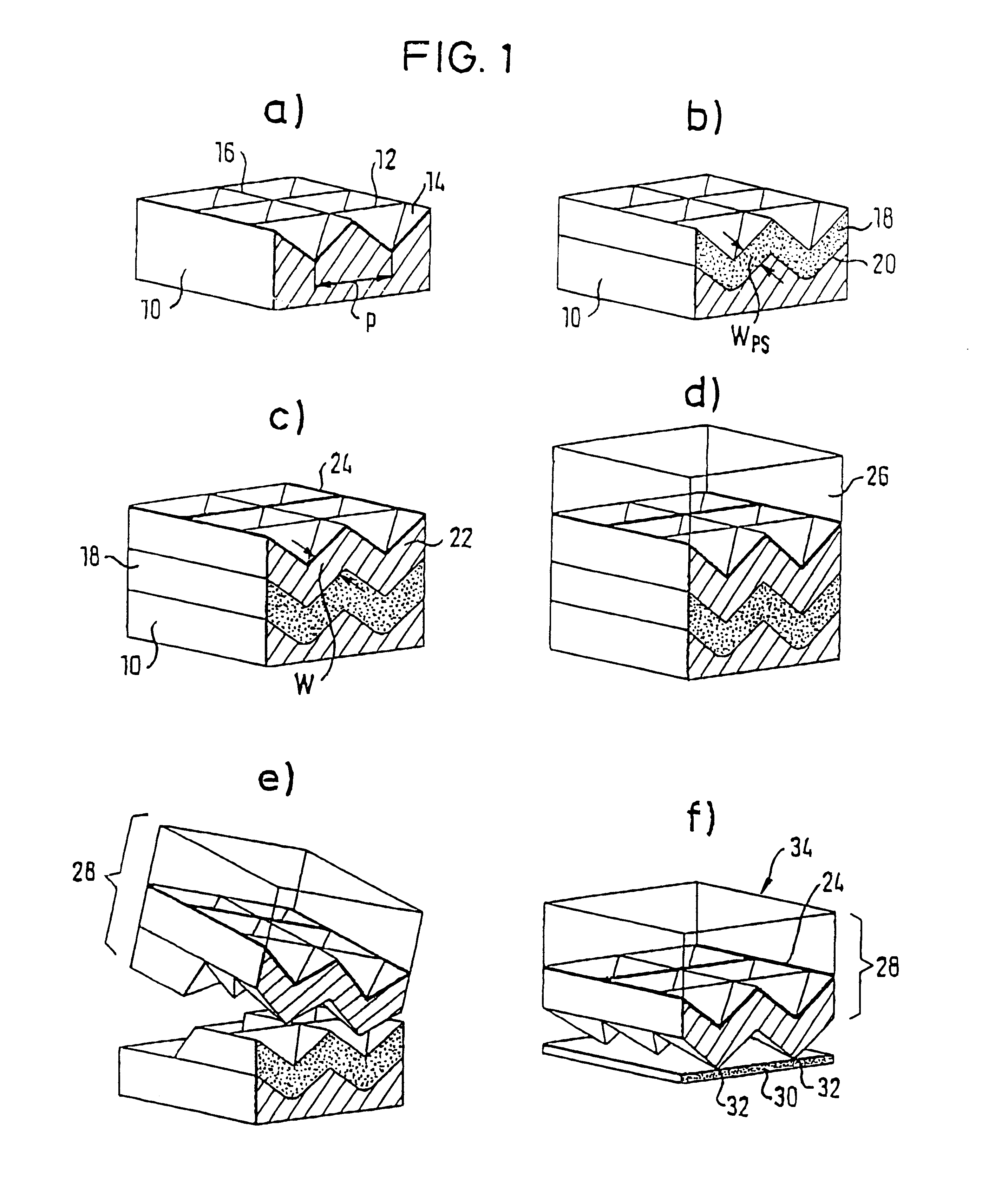
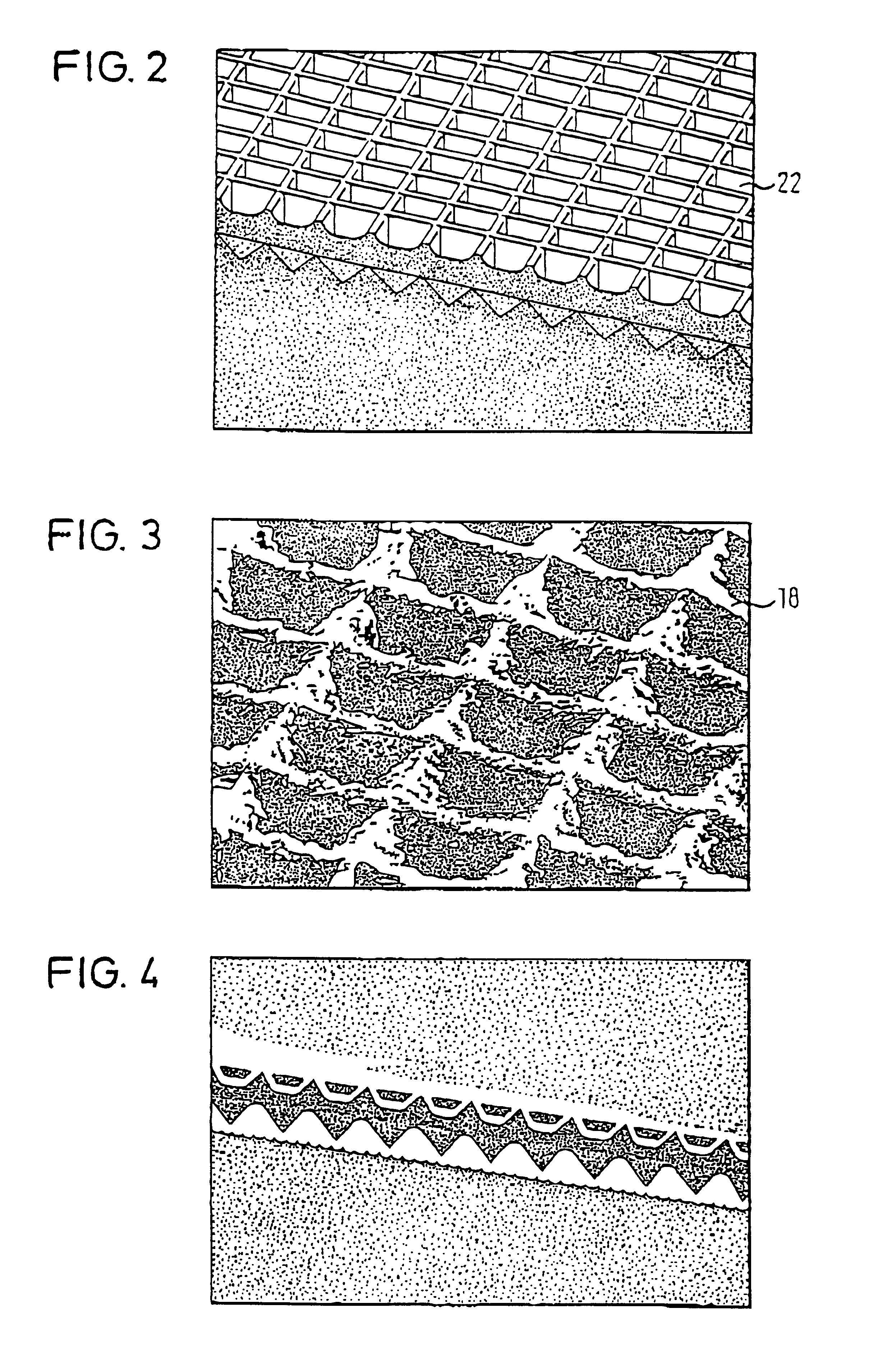
FIG. 1A shows a silicon substrate 10, for example of p-Si, with an n-Si substrate likewise entering into question. The one surface of the Si substrate 10 has a structuring 12 which one can consider as a matrix of pyramidal recesses 14, the base surfaces of which are placed directly alongside one another, so that the upper boundary of the surface is very similar to a square grid.

The substrate 10 is subsequently treated in manner known per se in order to produce a porous silicon layer 18 (FIG. 1B). The upper side of the porous silicon layer 18 has the same shape as the structured surface of the Si substrate 10. The boundary surface between the porous silicon layer 18 and the substrate has the same shape.

The substrate 10 is now coated by means of an epitaxial method. In this manner a layer 22 of epitaxial silicon first arises on the surface of the porous layer 18. In principle, any of the known epitaxial methods can be used for the formation of this layer 22, i.e. amongst other things ...


PUM

PropertyMeasurementUnit
porosityaaaaaaaaaa
porosityaaaaaaaaaa
porosityaaaaaaaaaa

Abstract

The invention relates to a method of manufacturing layer-like structures in which a material layer having hollow cavities, preferably a porous material layer, is produced on or out of a substrate consisting, for example, of monocrystalline p-type or n-type Si and in which the layer-like structure, or a part of it, is subsequently provided on the cavity exhibiting or porous material layer. The layer-like structure, or a part of it, is subsequently separated from the substrate using the layer having the hollow cavities, or porous layer, as a point of desired separation, for example through the production of a mechanical strain within or at a boundary surface of the cavity exhibiting or porous layer. The method is characterized in that the surface of the substrate is structured prior to the production of the porous layer, or in that the surface of the porous layer is structured.

Description

1. Field of the InventionThe present invention relates to a method of manufacturing layer-like structures in which a material layer having hollow cavities, preferably a porous material layer, is produced on a substrate consisting, for example, of monocrystalline p-type or n-type Si and in which the layer-like structure, or a part of it, is subsequently provided on the cavity exhibiting or porous material layer, and is subsequently separated from the substrate using the cavity exhibiting or porous layer as a position of intended separation, for example through the generation of a mechanical strain within or at a boundary surface of the cavity exhibiting or porous layer. Furthermore, the invention relates to different substrates which can be produced by this method and to novel semiconductor components which can be manufactured using the substrates of the invention.2. Description of the Prior ArtA method of the initially named kind is known from several documents.By way of example, a ...

Claims


Application Information

Patent Timeline
Patent Type & Authority Patents(United States)
IPC IPC(8): H01L21/70H01L31/18H01L21/762H01L31/06H01L31/068H01L31/0236H01L31/052B01J19/08C30B29/06C30B29/66H01L21/20H01L21/304H01L21/306H01L31/04
CPCH01L21/76259H01L31/0236H01L31/068H01L31/056H01L31/1804Y02E10/52Y02E10/547H01L31/02363Y02P70/50
Inventor BRENDEL, ROLF
Owner MAX PLANCK GESELLSCHAFT ZUR FOERDERUNG DER WISSENSCHAFTEN EV
Why Eureka
Try Eureka