Device and method for selecting power down exit

a technology of power down exit and device, which is applied in the direction of digital storage, generating/distributing signals, instruments, etc., can solve the problems of consuming a large amount of power in the internal circuit of the sdram, and requiring more time to reach to ensure normal operation of the devi

Inactive Publication Date: 2003-11-18
SAMSUNG ELECTRONICS CO LTD
View PDF4 Cites 157 Cited by
  • Summary
  • Abstract
  • Description
  • Claims
  • Application Information

AI Technical Summary

Problems solved by technology

In each of the above clock synchronization circuits, the operation of the clock synchronization circuit and the drive buffer necessary for fanning out the clock signal to the internal circuits of the SDRAM consume a large amount of power.
However, ...

Method used


Image

  • Device and method for selecting power down exit
  • Device and method for selecting power down exit
  • Device and method for selecting power down exit

Examples


Embodiment Construction

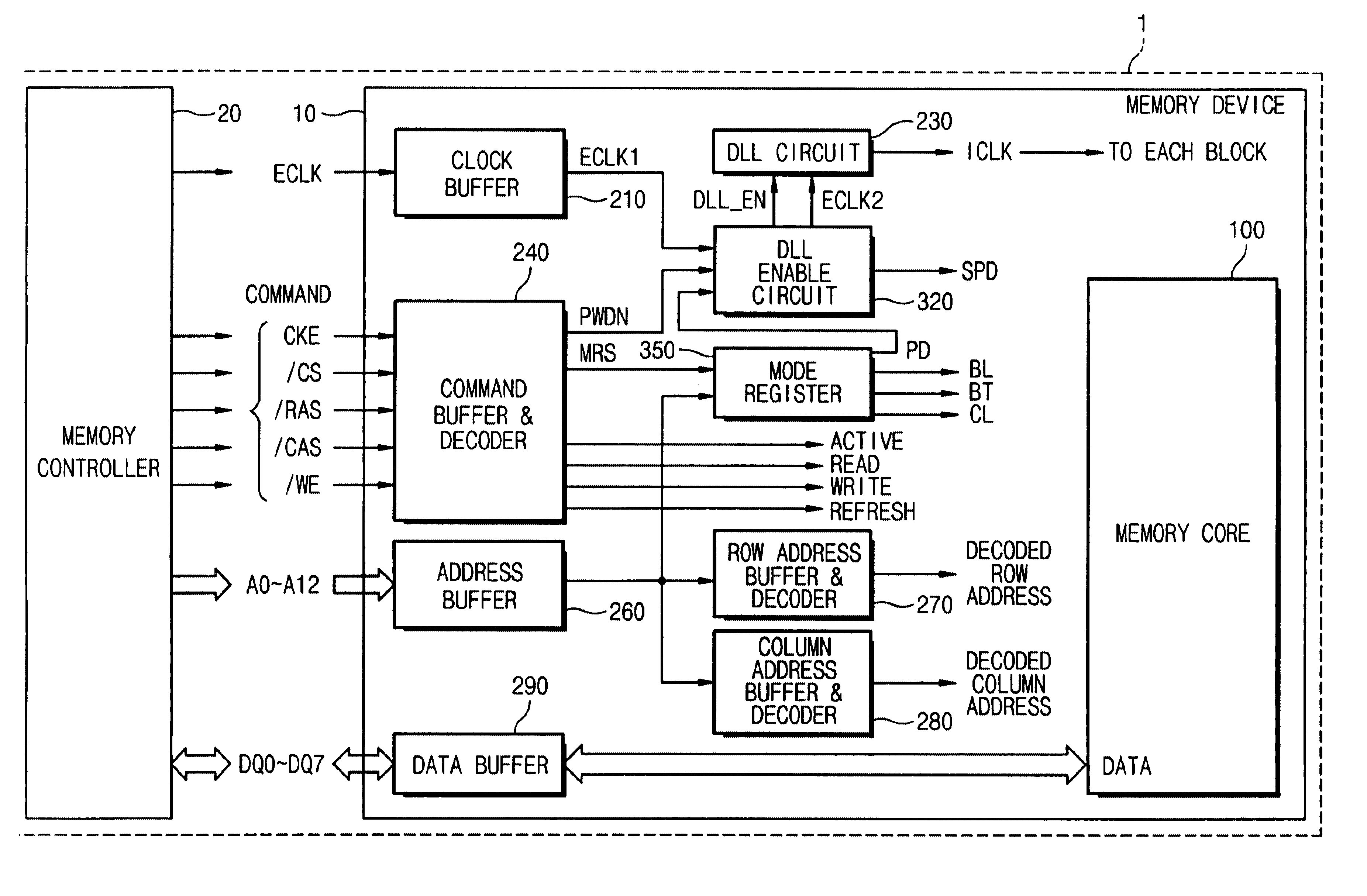
According to embodiments of the present invention, when a memory is exiting from a power-down mode to a normal mode, wakeup time and power consumption of the memory can be selected. The normal mode can be an active command, a read command or a write command. The selection can be based on power-down exit information stored in a mode register (MRS). If power conservation in an SDRAM is preferred, such as in mobile products, a slower wakeup but power-save mode is selected. If the memory (e.g., SDRAM) is employed in a high performance-computing device, where high-speed wakeup is preferred, a fast wakeup power-down exit mode is selected.

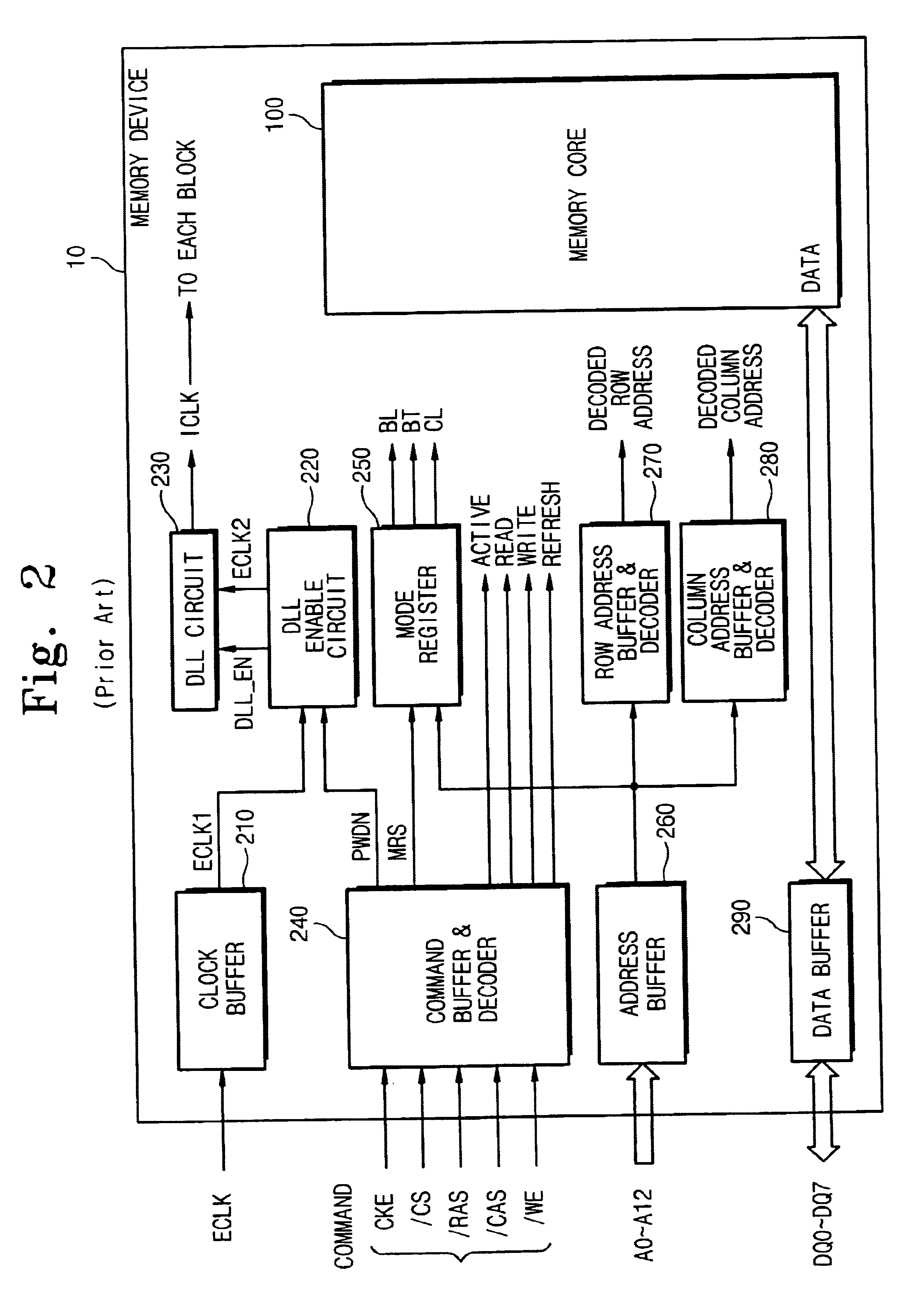
FIG. 4 shows a memory device according to an embodiment of the present invention. The memory device 10 comprises the memory core 100, which is a DRAM having an array of memory cells arranged in rows and columns. The DRAM is preferably an SDRAM or a DDR SDRAM. Row address buffer and decoder 270 and column buffer and decoder 280 provide the row addresses an...


PUM


Abstract

A semiconductor integrated circuit and a memory device capable of selecting power-down exit speed and power-save modes and method thereof are provided. The memory device includes a command decoder for generating a power-down signal in response to a power-down command, a mode register (MRS) for storing power-down exit information, a clock synchronization circuit such as a DLL or PLL circuit for generating an internal clock signal synchronized with an external clock signal, and a controller for controlling the DLL or PLL circuit. At power-down exit of the memory device, the power-down exit information can be selected between a fast wakeup time and a slow wakeup time.

Description

1. Technical FieldThe present invention relates to a device and method for controlling a semiconductor memory device and more particularly, to a circuit or memory device having a circuit for controlling a memory and controlling operations of the memory in selectable power down exit modes.2. Discussion of Related ArtAs operating speed and capacity of semiconductor memory devices continually increase, it is advantageous to incorporate memory control circuits such as a clock synchronization unit within the memory device. The clock synchronization unit is used for generating an internal clock signal in synchronization with an external clock signal such as a system clock. The internal clock is used to synchronously drive memory devices such as SDRAMs and DDR-SDRAMS. The clock synchronization unit can be a phase-locked loop (PLL), delay-locked loop (DLL), or duty-cycle correction circuit.A PLL circuit typically includes a phase detector, a charge pump, a loop filter, and a voltage control...

Claims


Application Information

Patent Timeline
IPC IPC(8): G11C5/14G11C7/10G11C7/22G11C7/00G06F1/04G11C8/00G11C11/401G11C11/407G11C11/4074
CPCG11C5/147G11C11/4074G11C7/222G11C7/22G11C8/00
Inventor LEE, JUNG-BAELEE, DONG-YANG
Owner SAMSUNG ELECTRONICS CO LTD
Why Eureka
Try Eureka